Motorola's Pioneering 8-bit 6800: Origins and Architecture
Part 1 of the story of Motorola's 8-bit microprocessor design
Why write about the Motorola 6800 (pronounced ‘sixty-eight hundred’)? For the generation that grew up with home computers in the late 1970s, the 6800 was the 6502’s slightly boring uncle. It was used in ‘grown-up’ devices, like cash machines, but it was slower, more expensive and generally less interesting than the 6502.
In reality, the 6800 was a highly innovative design that, just as much as competing products from Intel, represented a major step forward in making computing widely accessible to all.
Intel would eventually ‘win’ in microprocessors with the x86 architecture, and winners write the history, but Motorola deserves just as much respect as an early pioneer. This is probably why the 6800 came top of our poll of which 8-bit design to write about.
The story of the 6800 is also a story of how a corporation can develop innovative technology with enormous potential, only to self-sabotage and hand the advantage to a competitor. We’ll see how this happened in Part 2 of the story of the 6800. We’ll also discover that, remarkably, almost 50 years after its launch you can still buy the 6800 today!
For modern readers the name Motorola is probably most familiar as a brand of cell phones made by Motorola Mobility, now a subsidiary of Chinese multinational Lenovo. Cell phones combine digital and wireless electronics and the roots of Motorola Mobility are in Motorola Inc. which, for many decades, operated at the leading edge of both fields.
Motorola Inc, was founded as Galvin Manufacturing Corporation by the brothers Paul and Joseph Galvin in 1929. Early products included a car radio which was given the brand Motorola, combining ‘Motor’ and ‘ola’ used in other audio products such as the ‘Victorola’ phonograph or record player. The car radios became so successful that the company changed its name to Motorola in 1947.
By the early 1950s the future of electronics lay in the transistor and Motorola built its first manufacturing plant for transistors, at a cost of $1.5m, in Phoenix, Arizona. Dan Noble, Vice President of Communications and Electronics, wrote enthusiastically and prophetically, about the new devices in the company’s 1955 annual report:
"The word 'revolution' may not be too strong to apply to the change which will take place in electronic equipment of all kinds within the next five years. The development of the transistor and other semi-conductor devices will reduce the size of equipment, improve the reliability of operation, and substantially reduce the operational power requirements. Not only will transistors replace vacuum tubes in many electronic equipments, but they will make possible the development of new devices for instrumentation, metering, controlling, detection, communications, and computing.”
By the mid 1960s, under the leadership of Lester Hogan, Motorola was making a variety of transistors, other discrete semiconductors and integrated circuits in Arizona. Hogan would ‘defect’ from Motorola to Fairchild Camera and Instrument in 1968, to become Chairman and CEO. Taking eight of his Motorola team, nicknamed ‘Hogan’s heroes’, with him, Hogan would replace Robert Noyce, when Noyce and Gordon Moore left Fairchild to found Intel.
The loss of Hogan and much of Motorola’s senior semiconductor team was just one contributor to a turbulent time for the company’s semiconductor division. The industry was in the middle of a transition from Bipolar to MOS integrated circuits. And a number of competitors were appearing, including the ‘Fairchildren’, companies founded by former Fairchild employees, including, crucially, Noyce and Moore’s Intel.
In the midst of all this change at the start of the 1970s, it became apparent to Motorola’s, mostly new, senior management team, that a number of firms were working on the development of microprocessors.
Tom Bennett, who would become a key member of Motorola’s microprocessor team, had been introduced to the idea in the form of early sketches for what would become the first commercial microprocessor, the Intel 4004, by Intel’s Ted Hoff. Bennett had been working on calculators at Victor Comptometer in Chicago, when he’d been approached by Hoff to see if he would be interested in using the proposed Intel chip in new calculator designs.
Bennett joined Motorola in 1971 to try to help them enter the calculator business. It was soon clear to Bennett, and others, that the microprocessor had much wider application than calculators. It could solve lots of other problems that had previously needed custom, complex and difficult ‘random logic’ designs.
Bennett had responsibility development of custom chips for potential external Motorola customers. One of those chips was a custom microprocessor for Olivetti. Motorola won the design, but couldn’t manufacture the chip in the required PMOS (p-channel Metal Oxide Silicon) process. Instead the design had to be licensed to competitor Mostek, who were able to build it, and who launched it as the Mostek 5065. Bill Lattin would later describe Motorola at the time:
…we had a rotating set of management, and nobody ever seemed to stick very long, and nobody ever understood the technology very deeply, and that was a real problem, because not only were implanters expensive. You needed clean rooms. This was a very expensive operation. Motorola wanted to get in, but they were, you know, didn’t quite understand what it was gonna take to get in.
Motorola’s inability to manufacture the 5065 must have been embarrassing. Lattin, received a, typically direct, recruitment pitch from Intel’s Andy Grove, who had taught Lattin at Berkeley, quoted in Inside Intel:
‘Grove had a very abrasive style,' Lattin recalled. 'It didn't work well with me... The recruiting style was: Motorola doesn't have a chance - we're going to kick their butts.'
Lattin declined Grove’s offer. The 5065 saga possibly convinced Motorola’s management that they needed to sort out their manufacturing processes. It certainly gave members of the Motorola team valuable experience in designing a microprocessor.
Starting the 6800 Project
But was making a microprocessor worth the considerable investment needed? At first Motorola’s marketing department quoted expected sales of only 18,000 microprocessors over five years.
But Bennett and colleagues continued to look for sales opportunities. National Data Corp (NDC) presented a proposal that would have required 200,000 microprocessors. NDC was a ‘time-sharing’ company that saw the opportunity to use a microprocessor in terminals connected to their central system. Nothing came of the NDC project, but it showed the sales potential and provided the impetus to start a new project to design a microprocessor..
So a team was assembled in Phoenix, Arizona. Bennett would become chief architect of the project. He was joined by Jeff LaVell and Bill Lattin. Together they used data that LaVell had gathered from talking to potential customers, to devise a series of integrated circuit building blocks. These could be used to create a range of systems, with an emphasis on those that needed communications capability. The 6800 would be joined by chips that would provide memory (6801, 6802 and 6803), input and output capabilities (6820 ‘Peripheral Interface Adapter’ and 6850 ‘Asynchronous Communications Interface Adapter’) and even a modem chip (6860).
John Buchanan who would do circuit design and the layout of the 6800 and the other chips. Rod Orgill assisted Buchanan with analysis of the design and layout. Bill Mensch worked on the design of the 6820. Chuck Peddle joined the 6800 team in 1973, after the design of the microprocessor was completed but worked on the 6820 and then on the marketing of the designs. The final team remained small, with around seventeen members in total.
6800 Challenges and Innovations
To build the 6800 and the other members of the family the team had to get both the logic design and the fabrication technology working. On the logic design Bennett would describe the approach as follows:
My original plan for it was to basically use a PLA [Programmable logic Array]-type control. But we couldn’t get enough speed out of it. So if you looked at the chip, the top part of it is all ROM, which does the initial decode of the instructions, and then after that there was a state counter, and that state counter cycled through, depending on how many separate steps it took to get the instruction completed.
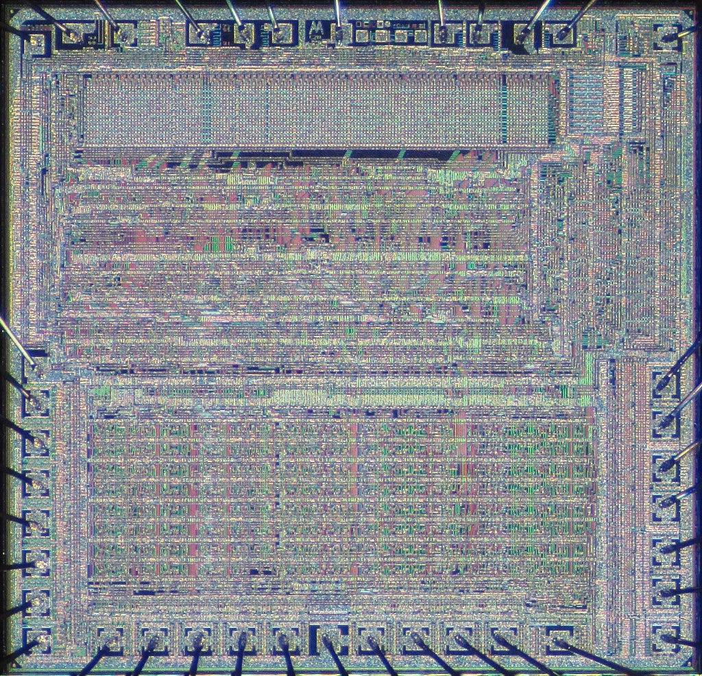
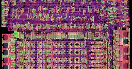
The layout of the 6800, with ROM at the top, registers and the arithmetic and logic unit at the bottom and control logic between the two can be seen in die shots and in the the ‘Visual 6800’ simulation, that shows how signals in the 6800 change as the 6800 runs (click on the picture below to see the 6800 in operation - highly recommended!)
On fabrication, the team made matters harder for themselves by aiming for a design that needed just a +5 volt input, unlike the +5,-5 and +12 volt inputs needed by competitors.
Launch and competition with Intel
Layout of the 6800’s design started at the end of 1972, but it took until February 1974 for the first parts, working apart from a few instructions with bugs, to be available.
The 6800 was announced in March 1974, just a month after Intel announced the competing Intel 8080. However, Intel had the 8080 in full production by April 1974, whilst the 6800 continued to be plagued by number of production issues that Motorola took several months to solve. The 6800 would only enter full production in November 1974, giving Intel a vital lead of a few months.
The 8080’s designer Federico Faggin later said:
Eventually, in the middle of 1974, the 6800 came out. That showed that our lead that was a year and a half was cut down by nine months. It was a major blow to me. But still, we maintained the lead.
... Motorola used a 5 volt process technology that was not ready for prime time, so their chip was very large and very slow. So it was not a match for the 8080, and that was actually what allowed the 8080 to gain market acceptance, despite the fact that, in my opinion, the 6800 had a better architecture. It was a more regular architecture. It did not suffer from this patch over the 8008 that the 8080 represented, and it had a better addressing mode. It was a nicer machine.
At introduction the 6800 was 29mm^2 and could only run at 1 MHz when compared to the 8080’s 20 mm^2 die size and ‘up to 2 MHz’ clock frequency.
Still, even if the 5 volt process wasn't quite ready, the simplicity of the design gave Motorola a key advantage.
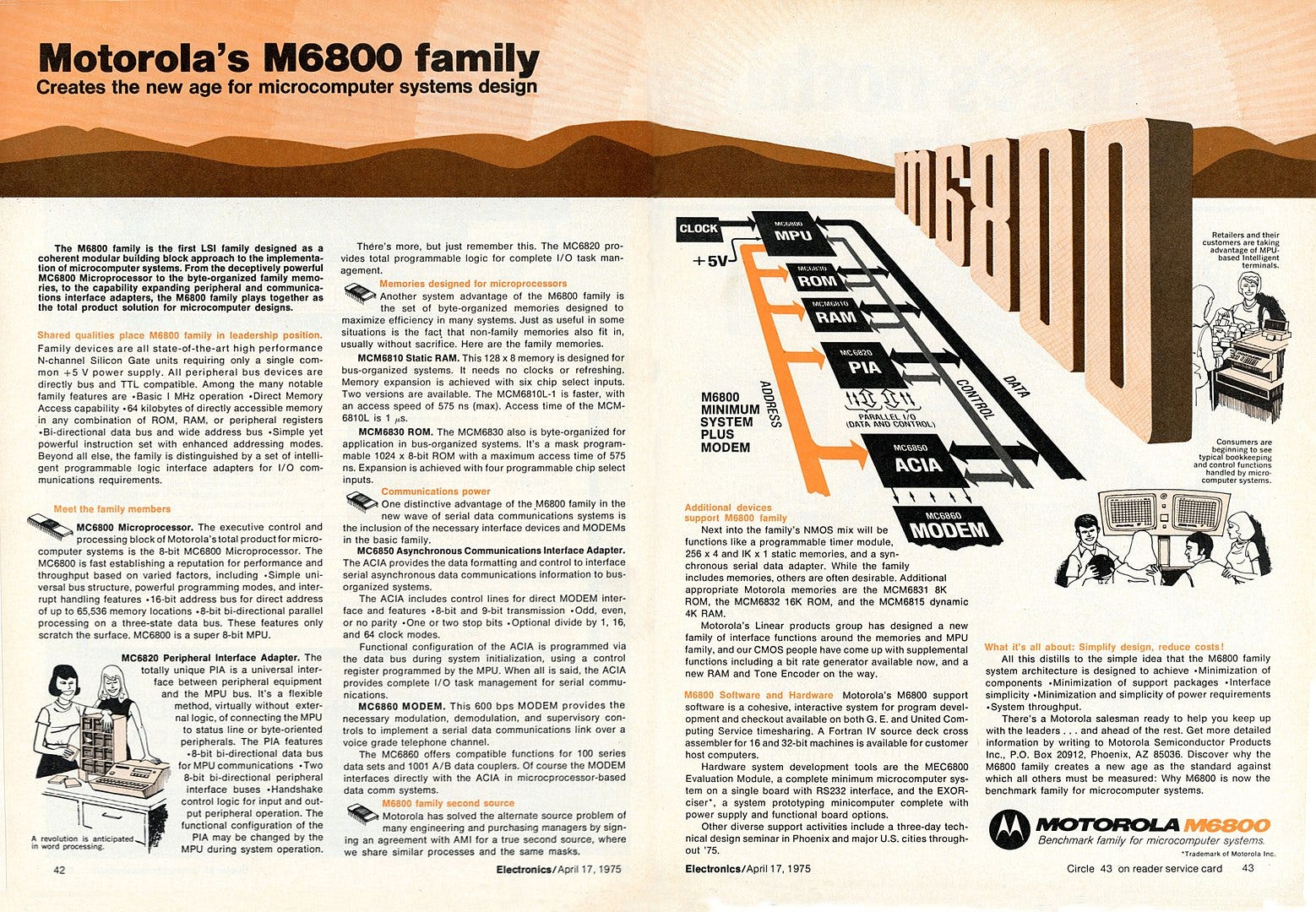
And the new Motorola family of chips was very capable. When the 6800 launched, the marketing material placed a lot of emphasis on the capabilities of the 6800 family of chips (known as the M6800 family) and on the communications capabilities of the family.
The M6800 family is the first LSI family designed as a coherent modular building block approach to the implementation of microcomputer systems. From the deceptively powerful MC6800 Microprocessor to the byte-organized family memories, to the capability expanding peripheral and communications interface adapters, the M6800 family plays together as the total product solution for microcomputer designs.
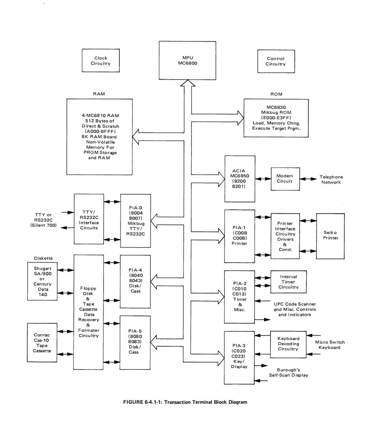
One notable feature of the M6800 family at launch was the quality of the documentation for the chips. Motorola’s 700 page manual for the system even showed how to use the 6800 family to create a complete ‘Point-of-Sale’ terminal.
So in the 6800 and the M6800 family, Motorola had a serious contender.
And it’s clear from the investment that Motorola’s management made in the project that they understood the importance of the 6800. An early 6800 development system was demonstrated to Motorola’s then CEO Bob Galvin, the son of one of the founders of the company.
It’s all the more surprising then that Motorola’s management should be careless with the team that designed the 6800. So careless, in fact, that their actions would lead to the creation of a new and powerful competitor to their new design. A competitor that would change the course of computing history. We’ll see how this happened in Part 2 of the story of the 6800.
The Architecture of the 6800
Unlike the Intel 8080, the 6800 wasn’t based on an existing microprocessor design. The Motorola design team largely had a ‘blank slate’, within the limitations of the technology of the time, so it’s interesting to look at their choices.
The 6800 design can be contrasted with the 8080. The Intel processor had lots of general purpose registers (A,B,C,D,E,H,L) some of which could be grouped to form 16-bit registers (BC, DE, HL). By contrast the 6800 had just two 8-bit accumulators (A and B) and a 16 bit index register (IX). Unlike the 8080, the 6800 had no 16-bit addition or subtraction.
The PDP-8 is often quoted as the model for the 6800, but it’s only a very loose model. The PDP-8 was a 12-bit machine, with a single 12-bit general purpose ‘accumulator’.
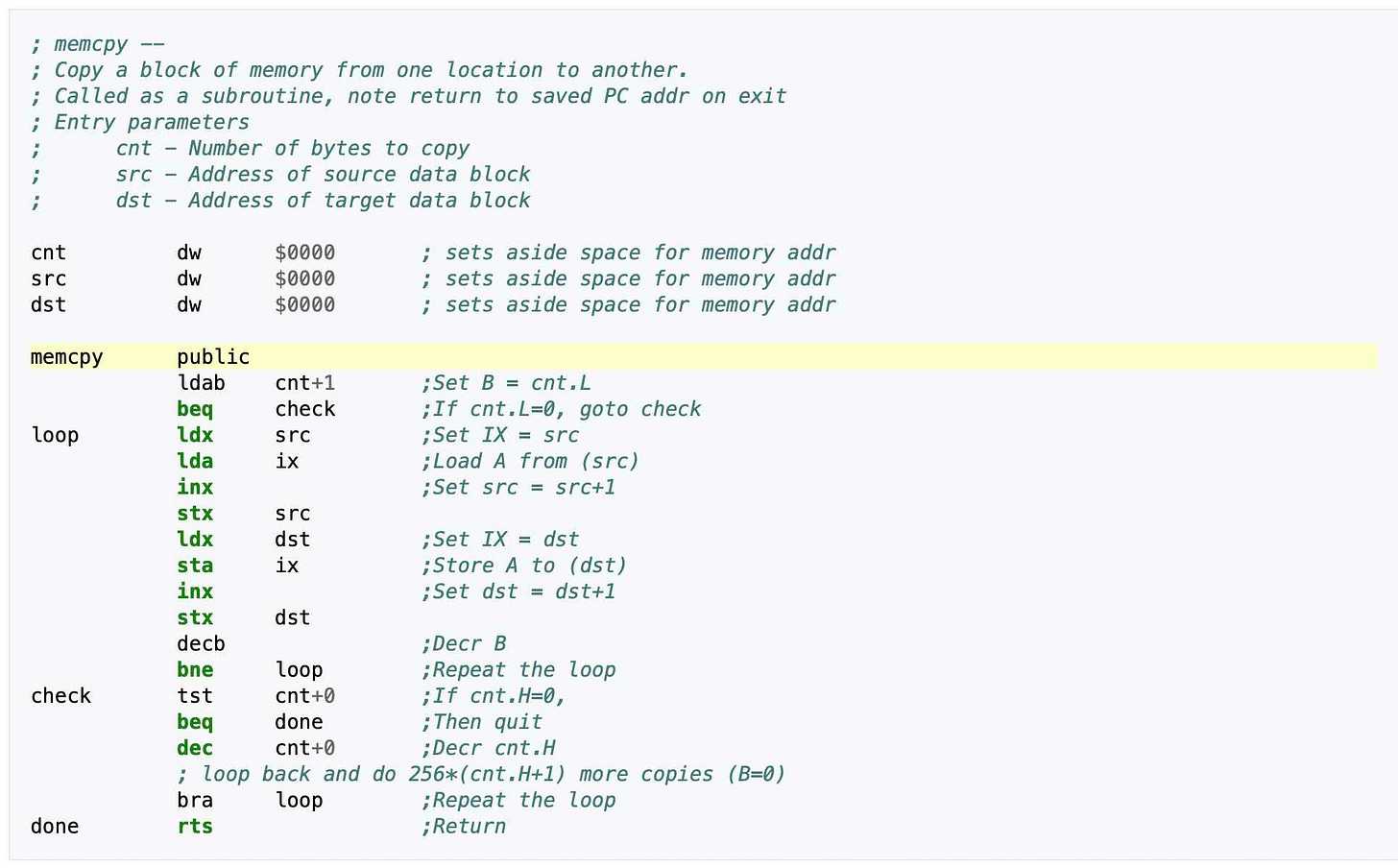
Wikipedia has some example 6800 assembly language code which shows off the general style and some of the weaknesses of the 6800. The sample code copies a block of memory from one location to another. The repeated 16-bit loads and stores from memory of the source and destination of the copy (using the index register ix - eg ‘ldx src’ ‘stx src’) is inefficient when compared to an architecture that could keep two memory addresses in registers at the same time. The 6800’s approach contrasts with the relative economy and efficiency of the same task on an Intel 8080, which makes use of the 8080’s multiple 16-bit registers.
Despite the lower clock frequency and smaller set of registers, there were ways in which the 6800 would outperform the 8080.
A simple instruction to load an 8-bit constant into the accumulator (‘MVI A, #FF’ in 8080 assembly language) would take 7 clock cycles in the 8080, whereas the corresponding instruction (“LDA A #FF” in 6800 assembly language) took just two clock cycles, meaning that even at half the ‘clock speed’ the 6800 would execute this instruction almost twice as quickly.
The 6800 also had some useful addressing modes. The indexed mode would add an 8-bit constant to the 16-bit index register to form a new 16-bit address, which could be used as a source for a load or an arithmetic, logic or compare instruction. Thus a single two byte instruction could perform an ‘add’ to create a new memory address and perform an arithmetic operation and all in just five clock cycles.
On paper the 6800 may have looked like it was, as Intel’s Faggin said, ‘very slow’, but Motorola would argue that it was ‘deceptively powerful’. The rivalry between 8080 derived and 6800 style designs would be a feature of the microcomputer market over the next decade.




If any DEC mini had influence on the MC6800 architecture, it was the PDP-11, not so much the PDP-8. The ONLY similarity to the PDP-8 is that both are accumulator-based architectures, while the PDP-11 has 8 general-purpose reisters. (Well, really 7, but who's counting.) Even there, the MC6800 is a bit closer to the PDP-11 by virtue of having TWO accumulators.
But the big similarity with the PDP-11 is the instruction set. The PDP-8 has only 8 instructions, none of which are very similar to the MC6800. The PDP-11 has a lot of instructions, and almost all of them have equivalents in the MC6800, even with related mnemonics.
A really Great Article on the Motorola 6800 Family.. Myself, as a Tandy Color Computer user since 2012 and a Tano Dragon Users since 2016, adding the Hitachi CMOS HD6309 is going another level in the MC6809 Family. Many people replace the MC6809 with the HD6309 because of the tremendous advancements available.. Advancements that Hitachi didn't tell Motorola about.. If you can, please add a Fourth Part to your series... https://en.wikipedia.org/wiki/Hitachi_6309