
Qualcomm's Hexagon AI Accelerators
Can Qualcomm’s smartphone NPUs give it an edge in AI datacenters?

This is a part free and part paid post. The first part, discussing Qualcomm’s recently announced AI200 and AI250 AI accelerators and the history of the Hexagon architecture is free, whilst the detailed look at the Hexagon architecture that follows is paid. None of what follows is investment advice.
You can upgrade to a paid subscription and support The Chip Letter using the button below.
“Qualcomm’s Hexagon might just be the most important architecture that no-one is talking about”
On 28 Oct 2025 Qualcomm announced two new data-centre AI inference servers, the AI200 and AI250. According to the press release:
Qualcomm AI200 and AI250 solutions deliver rack-scale performance and superior memory capacity for fast data center generative AI inference at industry-leading total cost of ownership (TCO). Qualcomm AI250 introduces an innovative memory architecture, offering a generational leap in effective memory bandwidth and efficiency for AI workloads.
Qualcomm also announced a partnership with Saudi Arabia’s HUMAIN to deploy its new data-centre technology:
Under the program, HUMAIN is targeting 200 megawatts starting in 2026 of Qualcomm AI200 and AI250 rack solutions to deliver high-performance AI inference services in the Kingdom of Saudi Arabia and globally.
The AI200 won’t be available until the end of 2026 and the AI250 until 2027 - an age in terms of the AI server market - and many are sceptical about Qualcomm’s chances of success in a market with lots of competitors. Qualcomm already has AI server products in the shape of the AI100 series and their lower cost cousins the AI80 series, announced as far back as 2019, which have made very little impression.
Despite all this the AI200 and AI250 announcements led to a pop in Qualcomm’s share price on the day.
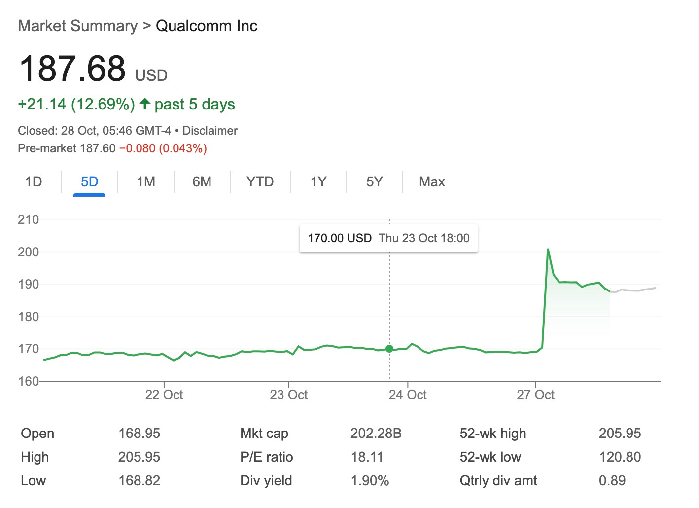
That’s an extra $20 billion or so in market value which seems a lot but is of course less than 1/2% of Nvidia’s market cap!
What is in the AI200 and AI250 to cause this excitement? Qualcomm are leading with ‘low total cost of ownership’ as the key selling point of the new designs.
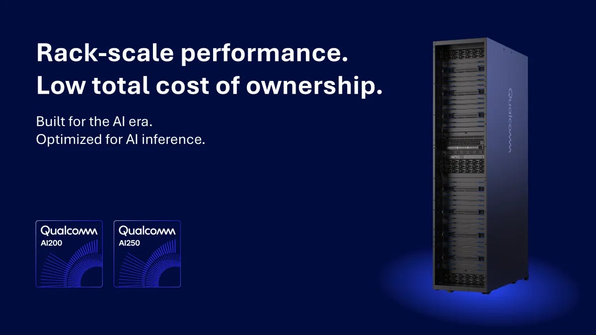
Part of this is probably Qualcomm’s use of LPDDR memory rather than the more expensive and scarce HBM. This should allow higher memory capacity - Qualcomm quotes up to 768GB per card - as well as reducing costs.

The idea of avoiding HBM isn’t new though, with Groq in particular apparently building a promising architecture and business on the concept.
SemiAnalysis drew out parallels with another chip giant.
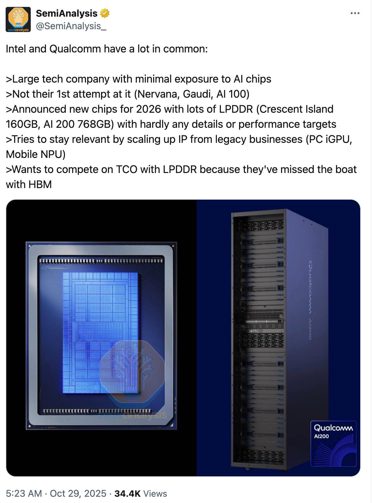
It’s fair to say that most of the reaction to the launch from commentators has been sceptical, to say the least. Here for example are SemiAnalysis again and Irrational Analysis.
Qualcomm has teased some more aspects of its new designs, including ‘an innovative memory architecture based on near-memory computing’, but there is a lot still to find out about what will power the AI200 and AI250.
For example, no CPU architecture was quoted in the announcement. Qualcomm has a very distinguished in-house CPU design team following its acquisition of Nuvia in 2020, a team that has since been put to work helping to create the Snapdragon X Elite series of Arm laptop System-on-Chips. Following its court win over Arm, Qualcomm is probably free to use the work of this team unencumbered. The original Nuvia designs themselves were high performance server CPU cores which might come in handy in ‘AI servers’.
As an aside it’s a bit uncomfortable to remember that Qualcomm has attempted entry into the Arm server market twice before only to abandon its efforts. On the second occasion, with Centriq, it didn’t even ship a single chip before giving up!
Probably more important than the CPU in the proposed AI200 and AI250 designs, though, is the ‘AI accelerator’ and here Qualcomm was more explicit, stating that the designs would be based on its existing Hexagon NPU designs:
NPU stands for ‘Neural Processing Unit’ which has become the established term for a dedicated (non-GPU) AI accelerator deployed at ‘the edge’: most likely in your recent smartphone, tablet or PC. I wrote a Q&A on NPUs last year that defined an NPU as follows:
An NPU is a specialised piece of hardware that’s designed to undertake certain AI or machine learning-related tasks. More specifically, it is specially designed to perform calculations needed for ‘inference’ or the application of an already trained deep learning model to generate useful results for the user.
Qualcomm and Hexagon NPUs featured in that post mostly in the context of Qualcomm’s laptop Snapdragon X Elite chips, but they feature heavily in Qualcomm’s Automotive platforms too:
The dedicated Neural Processing Unit (NPU), designed for multimodal AI, is designed to offer a 12x performance boost* over previous cockpit platforms, enabling real-time occupant data processing. This advancement facilitates live decision-making, adaptive responses, and proactive assistance, enabling personalized in-cabin experiences. Equipped with transformer accelerators and vector engines, along with mixed precision support, the NPU in Snapdragon Ride Elite is designed to deliver low-latency, highly accurate, and efficient end-to-end transformers, maintaining optimal power and performance.
The overwhelming majority of Hexagon NPUs, though, have shipped in smartphones using Snapdragon SoCs or in Qualcomm’s cellular modems used by Apple amongst others. In fact Qualcomm has shipped billions of Hexagon cores over the last two decades. Hexagon NPUs are, quite literally, almost everywhere!
It might seem strange to talk about “scaling-up” an accelerator from a smartphone processor. However, any processor designed for smartphones is likely to be designed for power efficiency. Power draw is now clearly a key constraint on the growth of AI datacenter.
Is it possible that, in the same way that the power efficiency of Arm CPU designs has helped to support the architecture’s entry into laptops, desktops and now servers, the power efficiency of Qualcomm’s smartphone NPUs will enable it to create a competitive server AI accelerator?
All this suggests three questions:
Are there any clues in Qualcomm’s existing Hexagon designs that might help us predict what is coming in the AI200 and AI250?
Is it just convenient for Qualcomm to use its existing Hexagon technology or will it give it a competitive advantage against other server accelerators?
Does the fact that Qualcomm has already shipped billions of Hexagon cores give it any advantages?
The rest of this post looks at the history of Hexagon and at recent versions of the architecture to see what we can find to try to answer these questions. Aside from its relevance to Qualcomm’s AI server prospects Hexagon is one of the most interesting architectures out there today. So it’s also a great opportunity to take a detailed look at possibly the most widely deployed NPU architecture. In fact, Qualcomm’s Hexagon might just be the most important architecture that no-one is talking about.
Hexagon’s Origins
Before the NPU there was the DSP:
There’s been at least one DSP [digital signal processor] core in every chip that Qualcomm’s ever made.
Qualcomm senior director of product management Rick Maule quoted in 2012
Qualcomm is synonymous with cellular (mobile) technology, which means modems, and a working modem needs compute. The nature of that compute, and the power constraints inherent in cellular designs, means that a general purpose CPU architecture such as Arm or x86 isn’t up to the task. Something more specialised, in the form of a Digital Signal Processor (DSP) is needed.
What is a DSP? By definition a DSP is designed to do ‘Digital Signal Processing’ but that doesn’t get us very far. Wikipedia provides a long list of DSP tasks, which seems almost too diverse to be helpful in pinning down what a DSP is designed to do:
DSP applications include audio and speech processing, sonar, radar and other sensor array processing, spectral density estimation, statistical signal processing, digital image processing, data compression, video coding, audio coding, image compression, signal processing for telecommunications, control systems, biomedical engineering, and seismology, among others.
It turns out that the DSP has been something of a chameleon, changing its colours and its uses, depending on the nature of the challenges that it’s been presented with. It’s probably more helpful to look at specific DSP designs rather than try to pin down a generic definition. In fact, as we’ll see Qualcomm’s DSPs have changed so much that Qualcomm isn’t calling them DSPs any more: they’ve evolved into a higher form of life in the shape of the AI-focused ‘Neural Processing Unit’ or NPU although it’s important to note that they still perform ‘DSP type’ roles.
Before we get to these NPUs, though, we’ll take a rapid tour of the history of Qualcomm’s DSPs, a history that starts soon after the firm’s founding, in July 1985, by Irwin Jacobs with six other former colleagues from Linkabit Corporation. In fact the story really starts at Linkabit with the Linkabit Microprocessor (LMP) a design used to decode signals from outer space:
Linkabit began by providing hardware and software to the Air Force that assured secure and reliable communications for targeting strategic (i.e. nuclear) … As part of its efforts to reduce the cost and size of the military communication devices, [klein] Gilhousen led the company’s successful efforts to develop one of the first digital signal processors on a chip, the Linkabit Microprocessor (LMP). In 1973, only two years after Intel released the world’s first microprocessor, the Intel 4004, Gilhousen began writing the microcode describing the operations of the LMP. With Sheffield “Sheffie” Worboys and Franklin Antonio, he completed a “breadboard” prototype of the new chip in May 1974. The microprocessor operated at 3 million cycles per second, or about 1/1000 as fast as today’s desktop computers. Later that year, Linkabit used the LMP to implement the Viterbi algorithm for decoding digital signals from outer space.
Source :Before Qualcomm: Linkabit and the Origins of San Diego’s Telecom Industry
The LMP wasn’t really a microprocessor as it was built with several chips, but it was pioneering both in its architecture and in how it was put to use:
Gilhousen, Sheffie Worboys, and Franklin Antonio completed a breadboard of the LMP using mostly TTL chips with some higher performance MSI and LSI commercial parts in May 1974. It ran at 3 MIPS. There were 32 instructions and four software stacks, three for processing and one for control. It was part RISC (before there was such a thing), part DSP.
What would the LMP be used for?
Besides the fact that the LMP worked so well, the reason for the intense USAF interest became clear in 1978. The real requirement was for a dual modem on airborne command platforms such as the Boeing EC- 135 and Strategic Air Command aircraft including the Boeing B-52. The solution evolved into the Command Post Modem/Processor (CPM/P), using several LMPs to implement dual full-duplex modems and red/black messaging and control, ultimately reduced to three rugged ½ ATR boxes.
Qualcomm’s first product was the Omnitracs satellite communications system for trucking companies, profits from which helped to fund the development of Qualcomm’s first cellular products including modems, hardware that converts data from digital to analogue formats (and vice versa) so it can be transmitted over radio waves. Those modems needed compute as part of this conversion process. Existing off-the-shelf Digital Signal Processors from Texas Instruments and Motorola weren’t up to the job so Qualcomm designed its own. Qualcomm’s first DSP was developed around 1988–1989 for their QCT-1 CDMA prototype cellular system. CDMA stands for ‘Code-Division Multiple Access’ and was the cellular technology that helped propel Qualcomm to prominence. The Acquired podcast tells the story of CDMA’s role in Qualcomm’s rise very effectively.
This prototype design evolved to form part of the design of MSM (Mobile Station Modem) chips that powered early Qualcomm CDMA phones. As MSMs became more sophisticated so did the DSPs that powered them.
Qualcomm DSP 💔 Intel
There is an interesting chapter in the story of Qualcomm’s DSPs when the designs were fabricated by … Intel.
In 1993 Qualcomm launched its CD-7000 ‘reference’ phone design, which was important in demonstrating the viability of CDMA phones.
The CD-7000 phone used had a 16-bit Intel 80C186 CPU (a successor to the 8086/8088 designs used in the first IBM PC and in many other designs) alongside its DSP, leading to an early, seemingly somewhat reluctant, collaboration with Intel:
The logical next step was to integrate the two, except … Intel was not in the intellectual property business. Intel denied Qualcomm’s advances at first. Under persistent nagging from its San Diego sales office, Intel’s embedded operation in Chandler, AZ learned all about Qualcomm, CDMA technology, and market opportunities before agreeing to provide an 80C186 core.
Converting the 80C186 design from Intel-ese to a more industry standard design flow proved difficult. Qualcomm had designed the MSM with high-level hardware description language (HDL) techniques that could be resynthesized on different libraries quickly, along with a simulation database and test vectors. It quickly became obvious that it was easier to move the Qualcomm MSM IP into the Intel design flow, and have Intel fab the entire chip. Qualcomm agreed. Intel was about to enter both the mobile business and the foundry business.
This would turn into another huge missed opportunity in mobile for Intel: Qualcomm would soon switch to Arm, announcing its first Arm license in 1999. That year Qualcomm’s MSM3100 modem was launched with an Arm ARM7TDMI core alongside Qualcomm’s QDSP2000 DSP core. Over time Qualcomm would become one of Arm’s biggest licensees shipping billions of Arm cores in its Snapdragon mobile SoC designs.
Early Hexagon
Development of Qualcomm’s DSP cores continued in the 2000s with work on the sixth version of the DSP architecture, QDSP6 v1, which would be branded as ‘Hexagon’, starting in 2004 with the first production cores shipped in 2007.
In 2011 alone Qualcomm shipped an estimated 1.2 billion Hexagon DSPs. In the same year it opened up the cores to user programming explaining that:
… the Hexagon Access program was started to allow customers to program the DSP and thus exploit the power and performance benefits of offloading the ARM cores for performance, reduced power dissipation, or concurrency requirements.
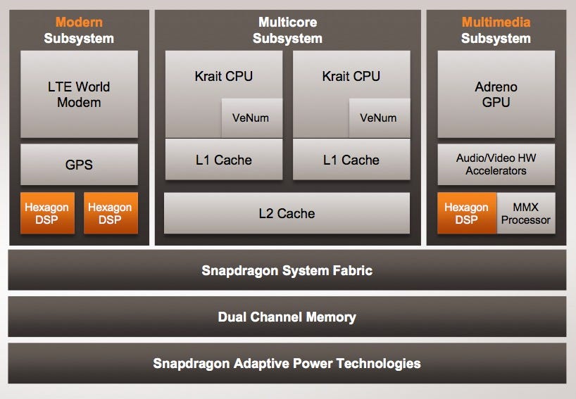
The Snapdragon 4 Plus SoC in 2012 had three Hexagon cores, two powering the modem and one, sitting alongside the Adreno GPU, MMX Processor and Audio/Video accelerators, in the design’s Multimedia Subsystem. This is all distinct from the, Qualcomm-designed Krait Arm cores.
Hexagon’s Route to NPU
With the increasing demand for multimedia tasks on smartphones the next logical step was to add vector processing capabilities to Hexagon. At Hot Chips in 2013, Qualcomm publicly announced the Hexagon Vector Extensions (HVX) targeting advanced imaging and computer vision workloads on the DSP.
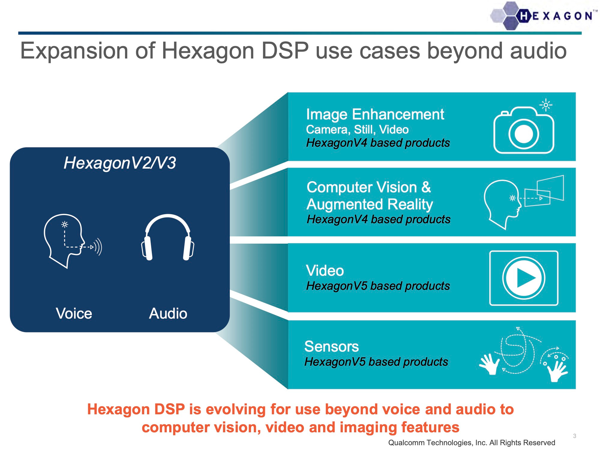
After vectors naturally come tensors - the generalisation of vectors - and the next major milestone in Hexagon’s evolution arrived with the Snapdragon 855 SoC in 2018. Integrated within its Hexagon 690 processor was a new, dedicated hardware block: the Hexagon Tensor Accelerator (HTA).
We’ll look in much more detail at modern Hexagon’s vector and tensor capabilities in a moment.
In the 2020s, with the excitement surrounding AI, when we discuss tensors we naturally think of neural networks and machine learning. It was inevitable that Qualcomm would eventually start describing Hexagon as an architecture for machine learning. So in the early 2020s the Hexagon DSP morphed into the ‘Hexagon Neural Processing Unit’ or ‘Hexagon NPU’ with the emphasis now on its ability to perform the processing needed for neural networks.
A brief aside. Given that GPUs are also commonly used for AI, readers might be wondering whether it’s possible to run user code - possibly for machine learning - on Qualcomm’s Adreno GPUs. It is, using OpenGL and Vulkan. However, Adreno cores do not contain tensor accelerators. It is possible to perform tensor-like operations but this is likely to be less efficient than using the Hexagon tensor units.
The Modern Hexagon Architecture
All this brings us up to date and to the modern Hexagon architecture. We’ve seen that Hexagon has evolved by adding vector and then tensor processing capabilities. It’s time to take a deep dive into how all these elements work together and how the Hexagon architecture differs from a typical CPU. For the rest of this post we’ll focus on recent Hexagon designs.