The next decade will see a Cambrian explosion of novel computer architectures, meaning exciting times for computer architects in academia and in industry.
John L. Hennessy and David A. Patterson (Turing Lecture, Communications of the Association for Computing Machinery, Feb 2019)
This post explores this Cambrian Explosion in hardware AI accelerators, perhaps aiming to reproduce some of the excitement that David Patterson refers to!
Please note that this is a long post (printed out it’s more than 50 pages) so to read it all you’ll need to view in your browser.
The complete post, with seventeen extra accelerator architectures, is for premium subscribers. Click on the button below to upgrade. Thank you!
Drawing an historical analogy to Helen of Troy—“the face that launched a thousand ships”—we say tongue-in-cheek that TPU v1 “launched a thousand chips.”
‘A thousand chips’ is obviously an exaggeration but the decade following the launch of Google’s TPU v1 in 2015 has certainty seen a lot of activity in the field of machine learning, and more specifically deep learning, accelerators.
This post aims to give a broad overview of activity in the field over the decade 2015 from 2023, by listing the most prominent accelerators developed over this period. There has been too much going on to claim to offer a complete list, with less emphasis on designs from outside the U.S. than is probably merited. I’m also sure that there are some architectures that are still ‘in stealth’ and not publicly described. There also isn’t space to go into depth on any single architecture. Instead we’ll provide just a few lines on each architecture with links for further viewing and reading. I’ve also saved the additions made to established CPU / GPU ranges, such as Tensor cores in Nvidia GPUs, for later posts. I’ve omitted the projects that are unlikely to be commercialised and designs mainly focused on inference at ‘the edge’.
I had a couple of objectives in writing this post.
To provide a (hopefully) helpful starting point for further exploration of AI accelerator hardware. To help with that exploration, there are links to presentations on each of the architectures listed.
To show just how much activity there has been on the development of AI accelerator hardware over the last decade or so.
It’s useful to group the activity in this field into a small number of categories:
TPU v1 and its Application Specific Integrated Circuit (ASIC) successors developed within Google;
ASIC’s developed by other hyperscalers or by established semiconductor or adjacent firms (such as Intel and Tesla);
ASIC’s developed by startups;
Machine learning accelerators added to existing CPU / GPU designs.
There is some overlap between these categories. For example, Intel has acquired multiple startups over this period. Some of the ASICs use established CPU ISAs (most notably RISC-V) extensively.
Omitting GPU designs leaves Nvidia, as the 800 pound gorilla of accelerated machine learning, out of the picture. One can sometimes feel the shadow of Nvidia’s presence in these designs, most obviously in the efforts by the hyperscalers to develop their own ASICs, which are probably, in large part, attempts to escape from (almost complete) dependency on Nvidia.
These ASIC designs have one thing in common. They all accelerate matrix multiplication using, from one (e.g. Google TPU v1) to very many, matrix multiply units. They differ in how these units are controlled, connected together, how large they are, their memory access, their software stacks and the business models for the companies that make them.
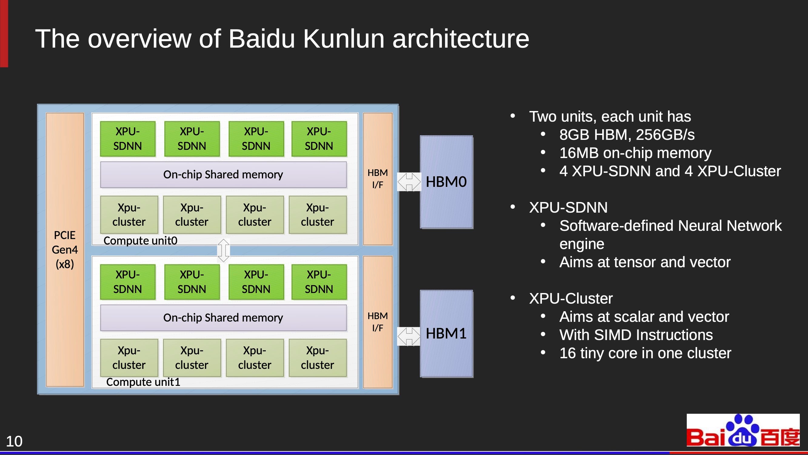
The chips / firms we’ll mention include : Google TPU v1-v5, Amazon Inferentium and Trainium, Microsoft Maia, Meta MTIA, Intel Nervana, Intel Gaudi, Alibaba Hanguang, Baidu Kunlun, Esperanto, Cerebras, Graphcore, Tenstorrent, Groq, SambaNova, IBM, Encharge AI, Moffett AI and more.
That’s a lot of chips but I know that it’s an incomplete list. Do let me know of interesting designs that I’ve missed!
Note that some of the most interesting designs are from the startups listed at the end of the post. It’s well worth browsing to the end.
It’s striking that almost all of this activity started well before the latest excitement (or hype, depending on your taste) with generative AI triggered by the launch of ChatGPT in November 2022. With further influx of interest and investment it seems certain that the list will grow and the capabilities of many of the designs here will expand substantially.
I suspect that most of these architectures won’t survive though. Some are almost certainly already doomed. The ones that survive are likely to be the ones that have a strategy to avoid the steamroller that is Nvidia, just like Arm avoided Intel in the RISC ‘Cambrian Explosion’ in the late 1980s and 1990s.
It’s just a subjective feeling, but it seems to me that we may have already moved on from the era that saw the conception and launch of these designs. In 2024 the stakes are higher and the focus has changed, for example to what can be achieved at Data Center level, as
The focus of the content linked to in this list is on architectures, so some brief words on three other key aspects of these designs: fabrication, deployment and software stacks.
Fabrication
Almost all of the designs listed here are fabricated by TSMC. Google’s TPU v1 used a 28nm process. More recent designs have typically used TSMC N7 or more advanced.
We have seen that (what is now) Broadcom provided substantial assistance to Google in building the TPU v1. They continue to support Google’s TPU efforts and also support other designs, including from other hyperscalers.
Software
On software the picture is complex and patchy. Most support use of one or both of Tensorflow and PyTorch. There isn’t space to go into detail on the software stack for each design but it’s interesting to see the varying emphasis on software in the presentations and supporting material.
Deployment
Where these designs are deployed, if at all, isn’t always clear. I’ve tried to highlight where they are available to access on public clouds.
Some points that jump out from this overview:
Interest in AI accelerators from Venture Capital has been substantial, as can be seen from the number of startups on this list.
Many, but not all, come from Silicon Valley. There has, of course, been strong interest from China for both commercial and political reasons. There are also designs from Toronto and the UK along with other locations in the U.S.
Many of these designs have attracted industry veterans such as Jim Keller at Tenstorrent and of course a number of members of the original Google TPU team. I suspect it’s not just the (potential) financial rewards but also the attractions of creating innovative designs.
This post links to over 10 hours of presentations on these designs. If you haven’t got time to watch them all then I recommend Jim Keller’s relatively short talk for a useful introduction to the issues and trade-offs in designing an AI ASIC, albeit with obvious bias towards the approach that his team at Tenstorrent have taken.
If you haven’t read them already and aren’t familiar with this area then it’s probably helpful to read the earlier posts on Google’s TPU v1 first.
Before we get started I do want to correct any possible misapprehension that the development of hardware machine learning accelerators only started in 2015. We can go back all the way to the Mark 1 Perceptron Machine, first announced to the world in 1958.
The Mark 1 Perceptron, being adjusted by Charles Wightman (Mark I Perceptron project engineer)
Over the following decades there have been many attempts, using a wide variety of approaches, to the challenge of accelerating the computations required to simulate neural networks. Many of the designs here adopt approaches that aren’t new. But mirroring the increase in interest in deep learning we have certainly seen a ‘Cambrian explosion’ of interest in hardware since 2015. Let’s start where this latest surge started: at Google.
The TPU v4 package (ASIC in center plus 4 HBM stacks) and printed circuit board (PCB) with 4 liquid-cooled packages. - By Norman P. Jouppi, George Kurian, Sheng Li, Peter Ma, Rahul Nagarajan, Lifeng Nai, Nishant Patil, SuvinaySubramanian, Andy Swing, Brian Towles, Cliff Young, Xiang Zhou, Zongwei Zhou, and David Patterson - https://arxiv.org/ftp/arxiv/papers/2304/2304.01433.pdf, CC BY 4.0, https://commons.wikimedia.org/w/index.php?curid=130427664
We’ve already covered TPU v1 in some detail in two posts. In this post we’ll just provide brief details of TPU v1 and its successors along with links to presentations that provide a lot more detail:
TPU v1
Introduced in 2015 (but announced in 2016)
Inference only
PCIe peripheral
DDR3 Memory
256 x 256 Systolic Matrix Multiply Unit (8-bit integer multiply)
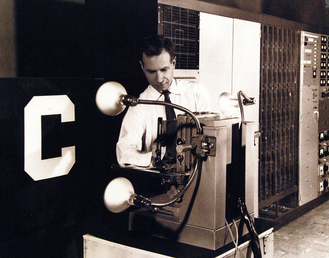
TPU v2
Introduced in 2017
Inference and Training
High Bandwidth Memory (HBM)
Two Matrix Multiply Units per chip using floating point (bfloat16)
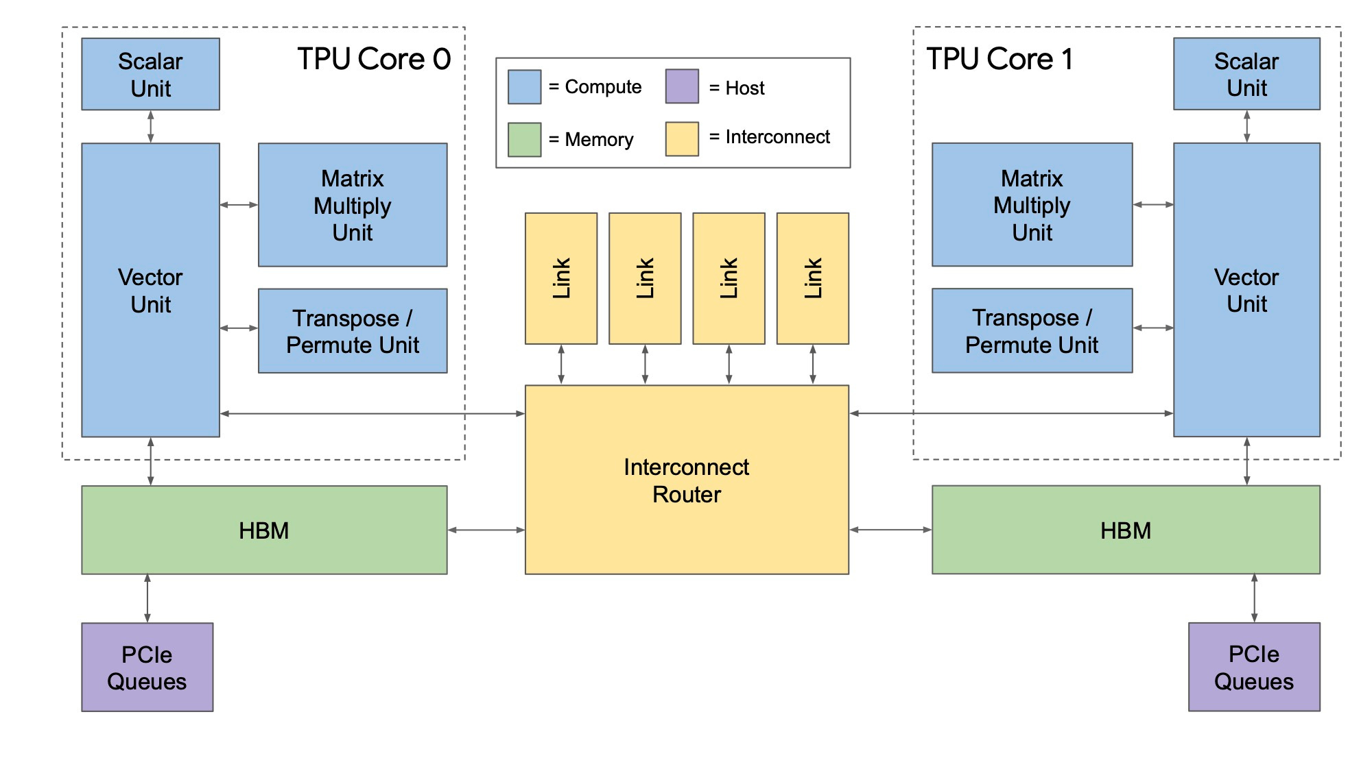
TPU v3
Introduced in 2018
As TPU v2 but with more memory bandwidth, higher clock frequency
Four Matrix Multiply Units per chip
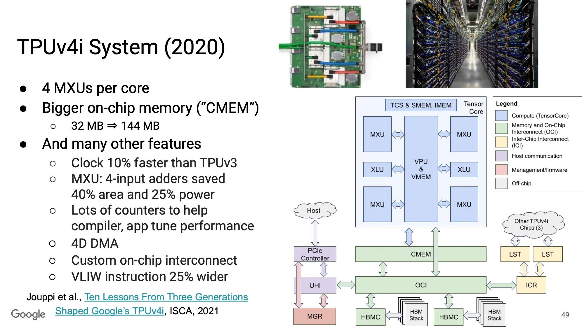
TPU v4 & TPU v4i
Introduced in 2021
Inference and Training (TPU v4) with liquid cooling or Inference (TPU v4i) with no liquid cooling
TPU v5p (performance) & TPUv5e (economy)
Introduced in 2023
“Designed for performance, flexibility, and scale, TPU v5p can train large LLM models 2.8X faster than the previous-generation TPU v4. Moreover, with second-generation SparseCores, TPU v5p can train embedding-dense models 1.9X faster than TPU v42.” Source
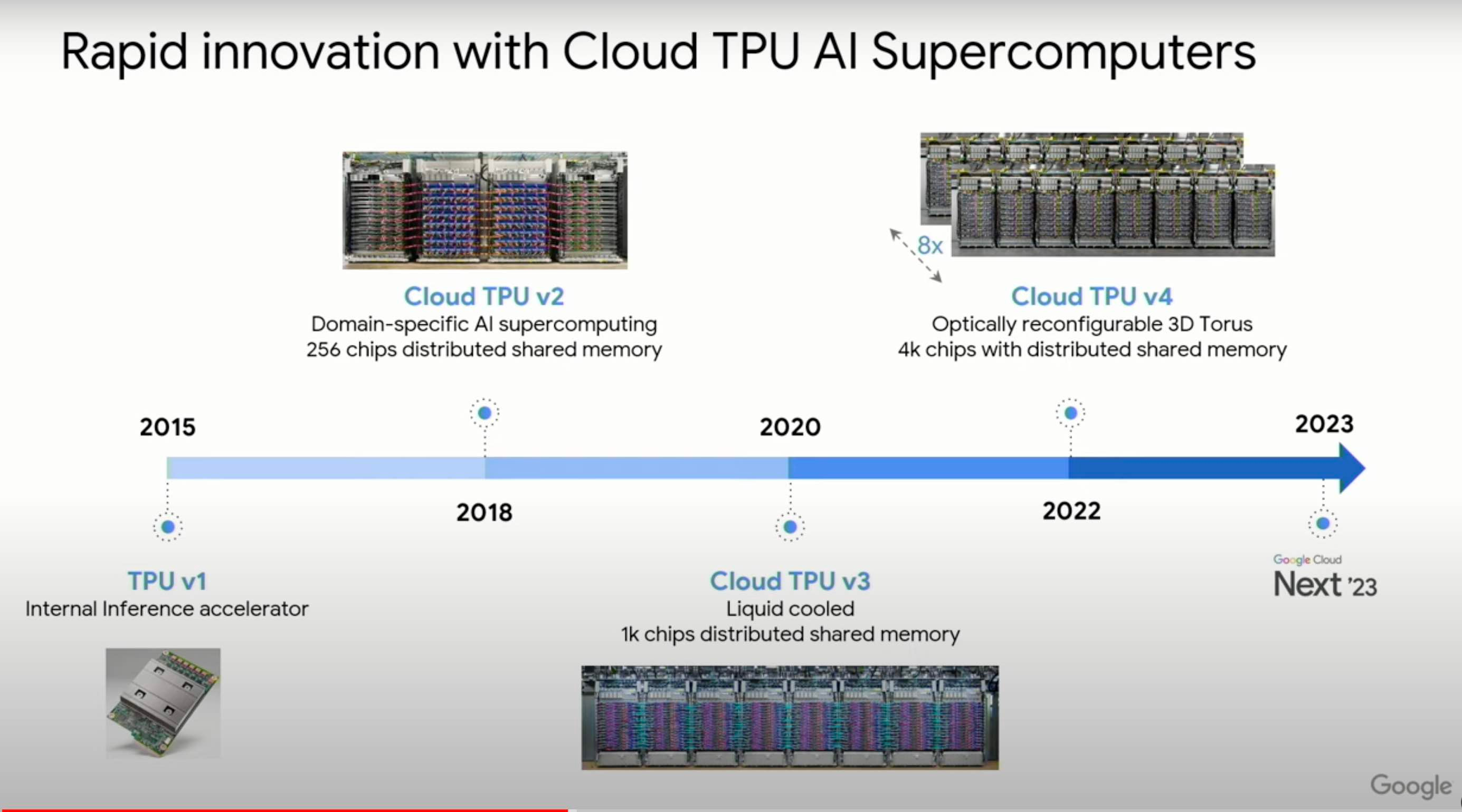
From Peripherals to Supercomputers
It’s interesting to see how focus in the TPU project has moved from creating a peripheral that can be attached to one of Google’s existing servers to ‘Cloud AI Supercomputers’ that can work independently and combine thousands of chips with shared memory and high-speed interconnect.
TPUs, VLIW and RISC-V
Readers may recall that TPU v1 used a CISC instruction set architecture with a small number of instructions.
The TPU has now changed to use a Very Long Instruction Word (VLIW) approach along with modified RISC-V cores from SiFive.
We’ll start with the ‘Hyperscalers’, like AWS and Microsoft, along with other semiconductor firms and established firms with an interest in machine learning.
Amazon
Inferentia & Trainium
AWS Inferentia accelerators are designed by AWS to deliver high performance at the lowest cost in Amazon EC2 for your deep learning (DL) and generative AI inference applications. (Amazon)
NeuronCore-v2 is the second generation of the NeuronCore engine, powering the Trainium NeuronDevices. Each NeuronCore-v2 is a fully-independent heterogenous compute-unit, with 4 main engines (Tensor/Vector/Scalar/GPSIMD Engines), and on-chip software-managed SRAM memory, for maximizing data locality (compiler managed, for maximum data locality and optimized data prefetch).
GPSIMD-Engine, which consists of eight fully-programmable 512-bit wide vector processors;
Presentations :
Microsoft
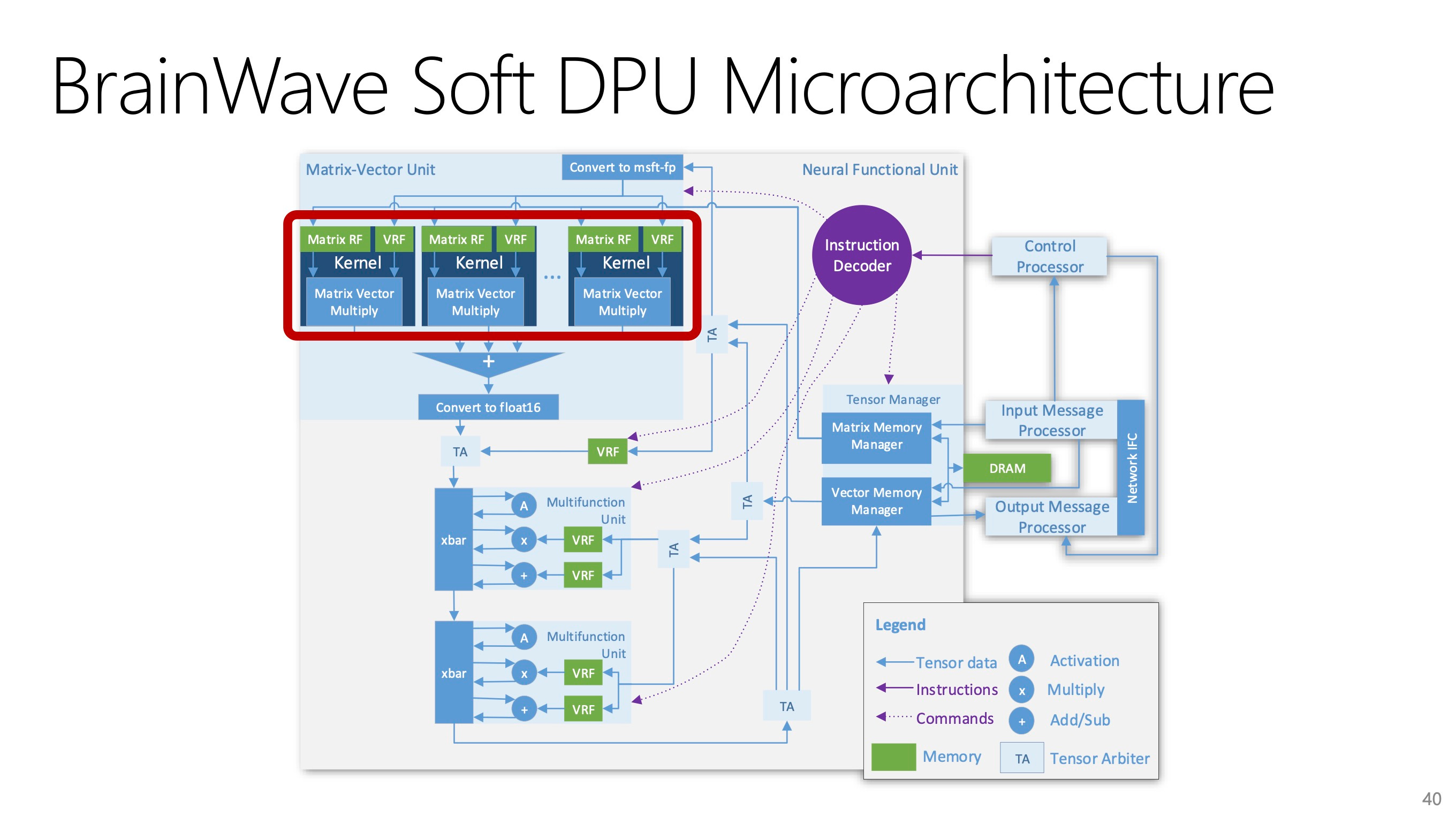
Microsoft’s original approach to machine learning hardware was to use Field Programmable Gate Arrays (FPGAs). Project ‘Brainwave’ implemented many of the features we have discussed already, on Intel FPGAs, in Microsoft’s cloud (see below for the Hot Chips 2017 presentation).
This approach changed last year when Microsoft announced Azure Maia.
Azure Maia AI Accelerator
The company’s new Maia 100 AI Accelerator will power some of the largest internal AI workloads running on Microsoft Azure. Additionally, OpenAI has provided feedback on Azure Maia and Microsoft’s deep insights into how OpenAI’s workloads run oninfrastructure tailored for its large language models is helping inform future Microsoft designs. (Microsoft)
In 2020, we designed the first-generation MTIA ASIC for Meta’s internal workloads. This inference accelerator is a part of a co-designed full-stack solution that includes silicon, PyTorch, and the recommendation models (Meta).