Demystifying GPU Compute Architectures
Getting 'low level' with Nvidia and AMD GPUs

The complexity of modern GPUs needn’t obscure the essence of how these machines work. If we are to make the most of the advanced technology in these GPUs then we need a little less mystique.
I think this is one of the most exciting times in computer architecture for many years. In CPUs we have x86, Arm and RISC-V, three increasingly well-supported application architectures.
And GPU architectures are, of course, becoming much more important. GPUs are obviously a critical piece of machine learning infrastructure. They are also making massively parallel computing available to help solve a wider range of computational problems outside of machine learning.
There is one problem though. How GPU architectures work is much less widely understood than is the case for CPUs. CPUs are often complex, but much of that complexity (pipelines, instruction and data caches, branch prediction, out-of-order execution, register renaming, virtual memory and so on) is largely hidden from the user, and can often be ignored. Doing things in parallel, though, is inherently more complex and GPUs necessarily expose a lot of complexity.
There is also a degree of mystique about GPUs. The recent (and excellent) Acquired podcast episode on Nvidia stated that for GPUs:
The magical unlock, of course, is to make a computer that is not a von Neumann architecture.
I know the Acquired hosts didn't mean to imply that GPUs are ‘magical’ but still the use of the word in connection with GPUs somehow seems appropriate. GPUs don’t use a ‘von Neumann’ architecture. Instead they use an unspecified, unnamed architecture, and if we don’t know what it is then its necessarily mysterious.
To make matters worse, there are several barriers to learning how GPUs work:
Architectural Variations: Each of the major GPU architectures has a somewhat different implementation.
Inconsistent Terminology: The major GPU designers use inconsistent terminology, both between themselves and with terms commonly used for CPUs. So a CPU ‘core’ is very different to Nvidia’s ‘CUDA core’.
Legacy Terminology: Some of the terms used are carried forward from the graphics origins of the GPU designs (e.g. ‘shaders’).
Software Abstraction: Some GPU complexity can be hidden from the user behind the abstractions used by software packages used to program GPUs. This helps when implementing programs, but sometimes it prevents users from developing an adequate picture of how the architecture works.
CUDA’s Dominance: Because Nvidia’s CUDA has been the market leader in GPU computing for many years now, the CUDA terminology tends to be used in many explanations making it hard to read across to other architectures.
No wonder it all seems a bit mysterious.
But as GPUs become more important, this seems like an unsatisfactory state of affairs. Let’s try to cut through the mystery!
This post started out as a history of the architectures used for general purpose computing on Nvidia GPUs. However, I quickly changed course for two reasons:
Just explaining one generation of architectures is complex. Attempting to describe a whole series of generations of architectures is complexity squared, and probably just too much!
There is already a awesome, detailed post by Fabien Sangland called A HISTORY OF NVIDIA STREAM MULTIPROCESSOR that sets out the history of the development of Nvidia’s GPU general purpose computing architecture over the period 2006 to 2020.
Just a word of warning about Fabien’s post though. It assumes a lot of prior knowledge about GPUs. Don’t worry if you don’t know what a ‘Streaming Multiprocessor’ is at this stage. All will, hopefully, become clear later! It’s worth scanning Fabien’s post, even if you’re not familiar with GPUs, to see how far Nvidia’s architectures have developed over this period.
Rather than repeat much of what Fabien has written, I decided that it would be more useful to provide a ‘ground up’ basic explanation of two recent architectures from Nvidia and AMD.
Before we move on though, I want to quote from Fabien’s post on how Nvidia’s general purpose compute architecture emerged:
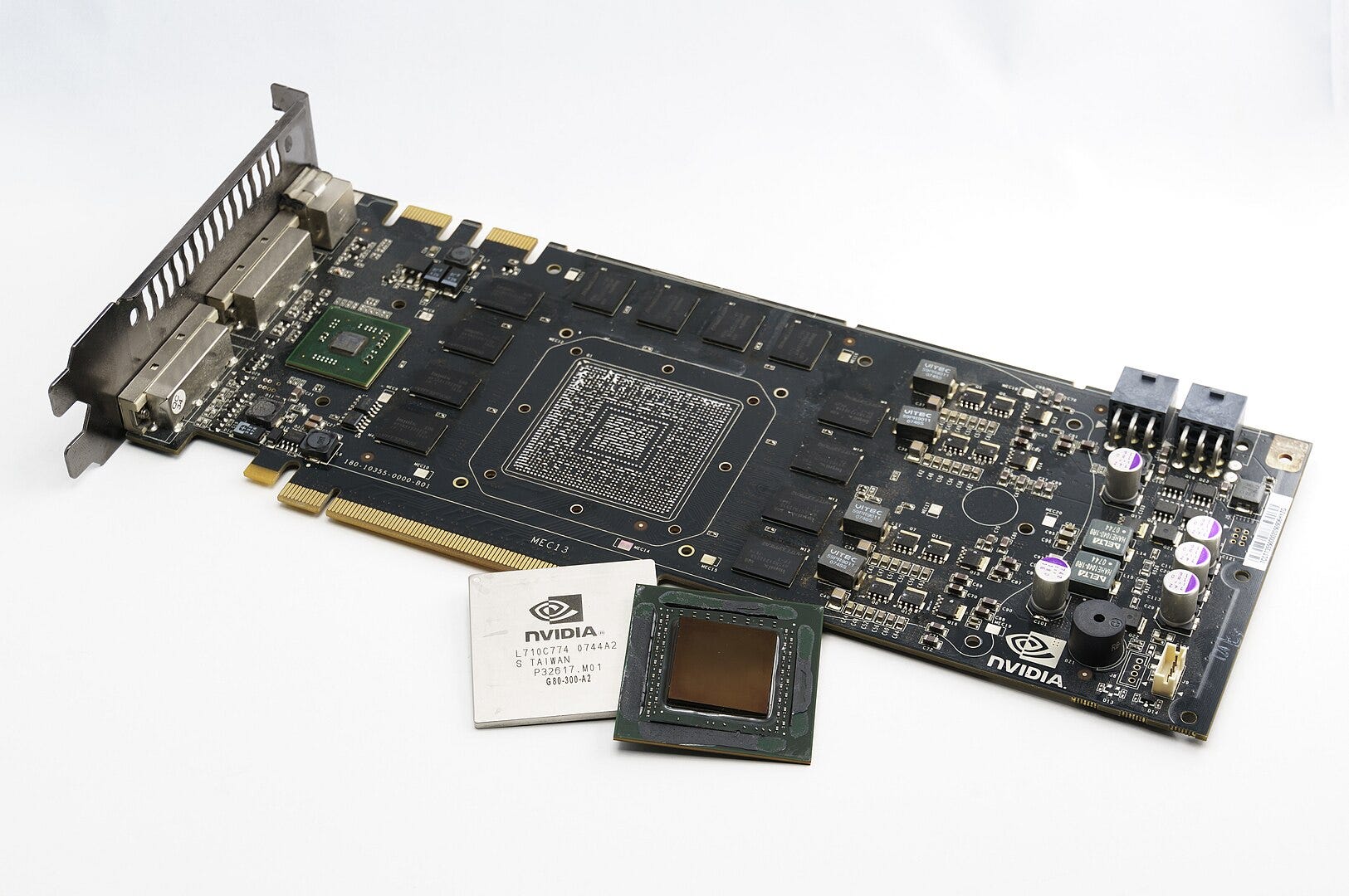
Up to 2006, Nvidia's GPU design was correlated to the logical stages in the rendering API. The GeForce 7900 GTX, powered by a G71 die is made of three sections dedicated to vertex processing (8 units), fragment generation (24 units), and fragment merging (16 units).
This correlation forced designers to guess the location of bottlenecks in order to properly balance each layers. With the emergence of yet another stage in DirectX 10, the geometry shader, Nvidia engineers found themselves faced with the difficult task of balancing a die without knowing how much a stage was going to be adopted. It was time for a change.
Nvidia solved the problem of escalating complexity with its "unified" Tesla architecture, released in 2006.
In the G80 die, there is no more distinction between layers. The Stream Multiprocessor (SM) replaces all previous units thanks to its ability to run vertex, fragment and geometry "kernel" without distinction. The load balancing happens automatically by swapping the "kernel" run by each SM depending on the need of the pipeline.
And so the first of Nvidia’s modern ‘general purpose compute’ architectures was born.
We pretty much threw out the entire shader architecture from NV30/NV40 and made a new one from scratch with a new general processor architecture (SIMT), that also introduced new processor design methodologies.
- Jonah Alben (Interview with extremetech.com)
And quoting Fabien again:
Tesla was a risky move which turned out to be a very Good Thing. It was so successful that it became the foundation of NVidia GPUs for the next two decades.
And we now how much of a ‘Good Thing’ this has been for Nvidia, which as I write this, has a $1.6 trillion market cap:
Nvidia has, by now, put in almost 18 years of development and investment, starting with the Tesla architecture, and including work on Nvidia’s famous ‘Compute Unified Device Architecture’ or ‘CUDA’ introduced in 2007. We’ve discussed some aspects of Nvidia’s strategy before (the first is now free to read):
The rest of this post explains how general-purpose computing on modern GPUs works ‘from the bottom up’. We’ll start at the lowest level, with two major architectures, and then build up from there.
I’ve chosen to look at both Nvidia (Hopper used in the H100 GPU) and AMD’s CDNA 2 (used in the Instinct MI200 GPU a version of which is used in Frontier Supercomputer) architectures and explain the common ground and the differences between these recent designs from each firm. We’ll focus particularly on clarifying some of the terminology used. We won’t consider the latest features built to accelerate machine learning, such as tensor cores. Instead, we’ll concentrate on the most ‘general purpose’ computing capabilities.
We will try to demystify the fundamentals of how modern GPU compute architectures work.
This is not a tutorial that will enable readers to get started writing programs on GPUs. Instead, if you want to do that, it’s intended as a supplement to help gain a better understanding of what is going on under the surface and the abstractions of a GPU program.
In any event, to properly understand a complex topic like how GPUs work, it’s really necessary to read lots of sources. To help with this, the end of this post has lots of references and links to further articles and presentations for readers who would like to learn more about GPU computing.
The aim is to help readers understand the fundamentals of GPU Compute Architectures without having to read a large manual. If you’d like to know more then read on!
GPU Compute Hardware
We’ll start by looking at GPU compute hardware. We’ll group into three ‘Levels’ - my terminology, in the absence of a common naming convention across architectures, and nothing to do with ‘Cache Levels’.
Level 1
We’ll start at the lowest level, with the basic building block of GPU architectures. Perhaps, surprisingly, this doesn’t seen to be given a memorable name by either Nvidia or AMD.
It contains a collection of compute resources that can perform a range of operations : integer, 32-bit or 64-bit floating point arithmetic, data loads and stores from or to memory and more.
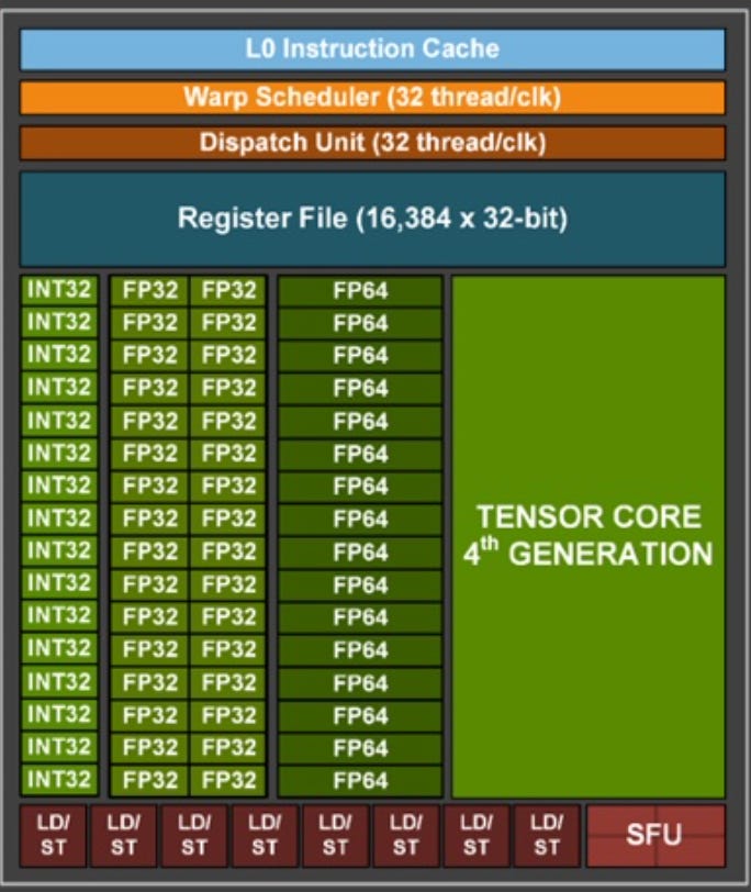
We’ll start by focusing on Nvidia’s hardware. Let’s have a look at a schematic of what this basic building block looks like. Here is a diagram from Nvidia’s Hopper H100 Architecture White Paper.
The smallest boxes here with “INT32'“ or “FP32” or “FP64” represent the hardware or ‘execution units’ to perform single 32-bit integer, 32-bit floating point or 64-bit floating point operations. So in this case we have thirty-two 32-bit floating point execution units, and sixteen each of the 32-bit integer and 64-bit float execution units.
As can be seen on the right there is also a ‘Tensor Core’ for the ‘tensor’ or ‘matrix’ operations required by many machine learning programs. We won’t discuss Tensor Cores further in this post.
At the bottom of this schematic are execution units (‘LD/ST’) to perform ‘loads’ and ‘stores’ from and to memory.
We need to consider how these execution units are controlled. Let’s focus on the integer and floating point hardware. The first thing to emphasise is that multiple execution units are grouped together and all execute a single instruction at the same time, so that their operation as a group is similar to how ‘Single Instruction Multiple Data’ or ‘SIMD’ operations work on a CPU. In fact GPU makers will sometimes refer to their architectures as ‘SIMT’ for ‘Single Instruction Multiple Thread’.
An instruction might, for example, perform a single operation on, for example, a ‘vector’ (or array) of sixteen 64-bit floating point numbers or thirty-two 32-bit floating point numbers or thirty-two 32-bit integers.
There are some differences when compared to SIMD on a CPU though. Unlike a modern CPU though, there are lots of features, such as branch prediction or out-of-order execution, that these processors don’t implement. This makes them poor as ‘general purpose’ processors. However, avoiding the complexity of these features frees up lots of space to squeeze in more of these processors on a single silicon die.
If they aren’t as efficient as CPUs at some things, they are much better at one task: switching between different programs. Without branch prediction, for example, programs running on this hardware are much more likely to have to wait for either program code or data to be fetched from memory. If this happens, then to keep the processor busy it can quickly switch to another program that is waiting and ready to take over. The ‘retired’ program can then be quickly restarted when it has the data that it needs.
We need a name for each of the elements of this hardware that operates on one item of data out of the ‘Multiple Data’ that it’s presented with. We’ll call this a ‘SIMT Lane’, analogous to a lane in a motorway, with multiple lanes laid out in parallel to allow multiple streams of traffic to progress at the same time.
Let’s cover the remaining features of this basic building block of GPU architectures.
There is some memory in the form of a ‘Register File’ and some ‘L0 Instruction Cache’ memory. We’ll come back to registers and memory on the GPU later on.
There is what is called a ‘Warp Scheduler’ and a ‘Dispatch Unit’. We’ll explain what a ‘Warp’ is precisely later on, but essentially this is hardware that organises the running of multiple programs on the execution units.
Finally, there is the ‘Special Function Units’ or ‘SFUs’ that can be seen at the bottom right. These execute transcendental instructions such as sin, cosine, reciprocal, and square root.
AMD’s CDNA 2 architecture hardware at this level is quite similar to Nvidia’s but with some differences.
For example it only has sixteen 32-bit floating point execution units. In most respects it operates in a similar way though. We’re not going to look at it in more detail at this point.
Level 2 - Streaming Multiprocessor (Nvidia) / Compute Unit (AMD)
The next stage in building the GPU is to group a number of these ‘Level 1’ hardware units together. Both Nvidia and AMD group four of these together in what they call either a ’Streaming Multiprocessor’ (Nvidia) or ‘Compute Unit’ (AMD) respectively.
Here is Nvidia’s schematic for a Streaming Multiprocessor. Nvidia also adds some ‘L1 Instruction Cache’ and ‘L1 Data Cache’. There is more on ‘shared memory’ later. We can ignore the ‘Tensor Memory Accelerator’ and ‘Tex’.
And here is a representation of AMD’s Compute Unit. AMD adds ‘Matrix Core Units’, more memory and a ‘Scalar Unit’, a scalar processor, which is distinct and runs independently of the other execution units.
‘Matrix Cores’ play a similar role to Nvidia’s Tensor Cores and are included to accelerate machine learning operations. We won’t discuss Matrix Cores further in this post.
Level 3 - GPU
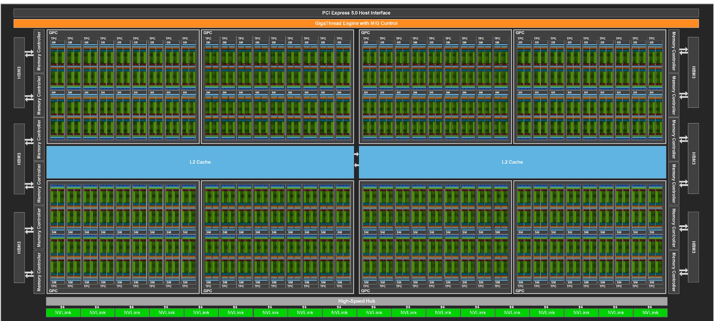
Our final stage is to bring together multiple Streaming Multiprocessors (Nvidia) / Compute Units (AMD) together. The latest GPUs from the two architectures each bring together more than 100 Streaming Multiprocessors / Compute Units.
Here is a schematic representation of the Nvidia H100 with 144 Streaming Multiprocessors per GPU (click for an easier-to-read version of this image):
And here is the AMD M200 with 112 Compute Units per GPU.
In each case the Streaming Multiprocessors / Compute Units are accompanied by ‘L2 Cache’ and by hardware to facilitate fast communication with other parts of the system (including memory). This hardware may use HBM, PCIe or proprietary technology such as NVLink (Nvidia) or Infinity Fabric (AMD).
Let’s briefly step back and consider just how much computational hardware one of these GPUs packs when compared to even the most powerful modern CPUs.
A leading AMD x86 CPU has 128 processor cores and has the floating-point execution units to perform (via AVX512 instructions) eight 32-bit floating-point calculations at a time. That’s 1,024 execution units per CPU. Contrast this with the 18,432 32-bit floating point execution units in Nvidia’s H100.
After the break we’ll discuss GPU instruction sets and registers, memory and software.


