Intel's Inside
The Early History of the Microcontroller Part 2
In which Intel uses its process and manufacturing leadership to create a winning proposition in the fast growing microcontroller market.
So here I am, I'm out of college a year, had a Bachelor's degree, thinking to myself what business do I have developing the next generation instruction set for these components? And really nobody was looking that carefully over my shoulder, but I said, okay, fine I'll go for it.
Intel’s Dave Stamm
Our next chapter in the story of the microcontroller sees a step change in the capabilities squeezed into a single-chip computer. With that we can see a corresponding step change in the range of applications where microcontrollers could be used. If there was a ‘microcomputer revolution’ underway in the late 1970s, then there was a parallel revolution underway based around microcontrollers, with computing power finding its way into a wide range of electronics for the first time. And much of that revolution had ‘Intel Inside’.
Today, we mainly think of Intel as a maker of powerful microprocessors for laptops, desktops and servers. But Intel also led the way in the early development of less powerful, but cheap and versatile, microcontrollers.
In Intel’s early years, its fabrication processes led the semiconductor industry, but its architectural efforts could be underwhelming. Intel’s first microprocessor, the 4-bit 4004. was an odd design. Its first 8-bit microprocessor, the 8008 was based on an architecture that was presented to Intel by a potential customer. The 8080 was a derivative of the 8008 and the 16-bit 8086 was, essentially, a much extended version of the 8080. Perhaps we shouldn’t be surprised. Intel was founded and led in its early years by a ‘trinity’ of leaders, Noyce, Moore and Grove, whose backgrounds were in physics and materials science, not computer architecture.
Its first microcontroller architecture was a design that has had much less attention over the years, but which quickly helped to establish Intel as a major player: the 8048 series. As we will see, the 8048’s architecture was developed by a tiny and very inexperienced team. It was flawed in some ways, but worked well enough for Intel to establish a big business around it.
In Tiny Computers from Texas, we saw how Texas Instruments built the first microcontroller, the TMS 1802NC, in 1971, to help the company more easily provide custom designs for its calculator customers. It had been a calculator maker, Japanese company Busicom, who had prompted Intel to develop the first commercially available microprocessor, the Intel 4004. Intel followed the 4-bit 4004 with the 4040 and then the 8-bit 8008 and 8080. Even as these more sophisticated microprocessor designs became available, Intel continued to sell the 4004 and the 4040 at lower prices.
But when TI launched the TMS 1000 microcontroller series in 1974, Intel’s 4-bit designs now had a formidable competitor. The TMS 1000 series packaged a 4-bit processor, RAM, ROM and input/output into a single package, which sold for less than $10. And it wasn’t just TI that was pioneering more powerful single-chip microcontrollers. Texas rival Mostek had also announced their own microcontroller product, the 8-bit MK 3870.
It was difficult for Intel, with its ‘multi-chip’ 4040-based solution, to compete with cheaper to use single-chip microcontrollers. Intel started to lose designs. The conclusion was clear. Intel needed its own single-chip microcontroller to compete with TI and Mostek.
EPROM’s Inside Intel
In the coming battle with TI, Intel was well placed. The company was growing rapidly and building a formidable reputation. According to Howard Raphael, one of the team that worked on the design of the new microcontroller:
... Intel had such a pizzazz; people were so interested in anything that Intel did because even then it was viewed as a technology leader. And Intel was very focused on microprocessors and memory that getting entrée into large customers was so easy.
And Intel had a crucial weapon with lots of ‘pizzazz’ in their fight with its competitors: ‘Erasable Programmable Read Only Memory’ or ‘EPROM’ invented by Dov Frohman1 in 1971.
Early EPROMs enabled users to erase the ‘Read Only Memory’ by shining ultra-violet light on the die. The chip could then be ‘re-programmed’ electronically and would retain the new data until erased again.
Frohman announced his invention in a way that must only have added to Intel’s reputation for ‘pizzazz’:
EPROM inventor Dov Frohman introduced EPROM's capabilities in a live demonstration at the International Solid State Circuits conference in 1971, using the bits of information on the chip to spell out the word "Intel." When he finished, the audience broke into applause.2
The first EPROM product, the 1702, was launched in 1972 with 256 8-bit bytes of EPROM memory.
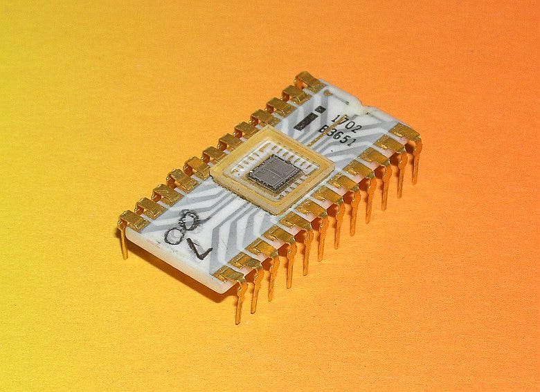
The 1702 exposed the surface of the die on the top of the package through a transparent ‘window’. Users could shine ultra-violet light on the surface of the die to erase it and then place the 1702 in a special circuit where it could be reprogrammed.
EPROM provided Intel them with an opportunity in the microcontroller market. Texas Instrument’s microcontrollers included some ROM but it was ‘mask programmable’. It could be changed only during manufacturing by altering one of the ‘masks’ in the fabrication process, which was both expensive and time-consuming. The high fixed cost of making a special mask also made the use of microcontrollers built in this way impractical in low-volume applications.
If Intel could build a microcontroller that replaced the ‘mask programmable’ ROM with an EPROM, then it had a compelling proposition.
Customers could start with an initial EPROM version of their design which they could easily debug and use to test in ‘real world’ applications, programming and then erasing and reprogramming themselves as necessary. If the application was low volume then they would continue to use the EPROM version in production. If the application was high volume they could transfer the code they had developed on EPROM to a mask-programmable version that Intel would produce more cheaply at high volume. It wouldn’t matter if the EPROM version was relatively expensive. It would be worth the price for customers to accelerate their development work and avoid the risk of having to rework an expensive mask-programmed version.
From Intel’s perspective, this would make the most of the limited resources that they had to build new masks needed for mask-programmable versions of the design. Now Intel would only be making masks for designs that would be going into high-volume production with code that had already been debugged by customers. A real bottleneck in the design process had been removed.
So initial work on new Intel microcontroller designs, which would become known as the MCS-48 or 8048 series, started in a group led by Ted Hoff, who had earlier started the project to build Intel’s first microprocessor, the 4004, and Sam Schwartz. One of their first decisions was to incorporate EPROM in the first version of the new design.
And it was perceived that, number one, the 8748 [the version of the new microcontroller series with EPROM] should be the first product because it put forth Intel's best technology …
Architecture
Intel needed an architecture for the new design. One option would have been to put the 4040 and its companion chips onto a single die. Intel and its customers could have re-used designs and code they had already developed. But the 4004 and 4040 had unusual architectures, tailored to meet the needs of the original Busicom calculator. There was no compelling need for backwards compatibility, so it made sense to move to something better.
The group under Hoff and Schwartz decided on a Harvard architecture, with address and data spaces distinct. But would the new design be 4-bit or 8-bit? Intel’s existing microcontrollers were 4-bit, as were TI’s competing designs. But an 8-bit design would open up a whole range of new applications that would not be possible with a 4-bit design. In the end, Intel’s senior management, in the shape of Ed Gelbach, made the decision.
We really couldn't decide whether it was 4-bits or 8-bits, so we set up a task force to make that decision. It turned out the task force got overruled by Ed Gelbach saying 4-bits didn't have enough sex appeal.
The second crucial architectural decision was that there would be two versions of the new series. The Intel team saw the need for microcontrollers that would themselves act as ‘intelligent peripherals’ in a larger computer system. These designs would share the instruction set of the wider 8048 series but other aspects of their design would be tailored to their specialized role.
Building the 8048
A group of just three engineers, Howard Stamm, David Buddy and Dwayne Hook, were assigned to work full-time on the new design. They started work in the basement of Intel’s, still new but already crowded, offices at Bowers Avenue. Stamm had been enthusiastic but soon realized what he had taken on:
… this is going to be technically a very difficult project because not only do we have to build a new instruction set, a new architecture, logic design using a technology that was designed for EPROMs and incorporate that all on one chip …
It was natural for them to try to make the most of Intel’s existing expertise in processor design. But that expertise was less valuable than they initially thought. They had to start from scratch with the logic design of the processor that would be built into the new microcontroller:
…basically there were no design libraries to work with. It was all on a blank sheet of paper.
Federico Faggin, who had led the design of all of Intel’s earlier microprocessors, had already left to found Zilog. Fortunately, Masatoshi Shima, who had worked closely with Faggin on all those designs, was still, for the time being, at Intel. Stamm has recalled how he would consult Shima:
I took Shima, who developed the early microprocessors […] I took all of his designs -- there was no full documentation pack in those days -- I just took them home and I went over every single circuit, every design, and just poured over all of his schematics, and then I would go back to him and ask him a few questions. So my learning process was just studying other people's designs. That was the only way there was to do it at the time, and Intel was on the leading edge of it, so where else could I go? That was the only place.
The fabrication of the new designs meant that they had to work closely with Intel’s process engineers.
So we were working on getting a denser technology, a 5 volt only technology, and buried contacts and depletion mode transistors so it would work with 5 volts, at about the same time. So we worked very closely with the group. Our mask designer laid out the first test chips for the process. So we had a very intimate working relationship with the process people at the time. It was a beautiful working relationship.
8048 Development
In the ‘team of three’ working on the 8048, Dave Stamm was in charge of development of the instruction set. Adopting a Harvard design, with separate instruction and data address spaces, meant that compatibility with Intel’s existing 8-bit microprocessors wasn’t an option. So Stamm largely had free reign to design a new instruction set. The main constraint was the restricted die area that would be available after the inclusion of EPROM, RAM and I/O. Stamm has talked about his lack of experience when he started to work on the 8048:
So here I am, I'm out of college a year, had a Bachelor's degree, thinking to myself what business do I have developing the next generation instruction set for these components? And really nobody was looking that carefully over my shoulder, but I said, okay, fine I'll go for it. Luckily in college I had taken assembly language programming in a language called COMPASS, which was part of CDC, which is no more. But I learned a lot about assembly language programming there, and then I'd worked on the 4040 and I looked at all the other instruction sets in order to try to come up with what kind of instruction set might make sense.
Stamm identified features in the instruction set that could be added or removed to keep the die area down:
There would be no arithmetic unit for subtraction and so no ‘subtract’ instructions;
Jumps in programs were all to absolute addresses with no relative jumps;
Memory was limited to 4k and was arranged into two 2k memory ‘banks’ with a RAM bit that determined which bank would be accessed.
However, even with the limited space available on the die Stamm managed to create an ISA with over 90 instructions, including some that were quite complex such as an ‘indirect jump instruction’:
A single byte indirect jump instruction allows the program to be vectored to any one of several different locations based on the contents of the accumulator. The contents of the accumulator points to a location in program memory which contains the jump address. … This instruction could be used, for instance, to vector to any one of several routines based on an ASCIl character which has been loaded in the accumulator. In this way ASCIl key inputs can be used to initiate various routines.
The original version of the ISA included the ‘SEX’ and ‘SIN’ instructions for ‘Set EXternal mode’ and ‘Set INternal mode’. Despite Ed Gelbach’s call for more ‘sex-appeal’ these instructions would be renamed with less salacious mnemonics.
With the ISA defined the team started to build a ‘breadboard’ with the design constructed using medium-scale integration TTL and DTL (Transistor to Transistor Logic or Diode to Transistor Logic) chips:
... we built this large breadboard, which in and of itself was yet a whole other design project, using the same type of combinatorial logic that we were hoping to eliminate through the development of the 8048. So we were using TTL and DTL devices. And the breadboard was huge as I recall. It was probably five foot tall by two or three feet wide, just completely covered with wiring on the back.
With a working design on the breadboard, the team created a chip ‘layout’ by hand on sheets of polyester film, known as mylar, and then transferred this to sheets of rubylith3 which would then be photo-reduced to create photo-masks.
Launch
By mid 1976 the team had working silicon which they could compare with the TTL breadboard they had used earlier in the design process. They were soon ready to share details of the new designs with potential customers:
We had certain customers we were showing the preliminary information on this product to, to see if they liked it. I recall showing the instruction set to some customers. … They were much more interested in the performance and the price of the product. And there was no question about it. The definition of the 8048 exceeded marketing's requirements because it had everything - it had a lot of things that the 4040 didn't have.
The new design was launched in the last quarter of 1976. The series of microcontrollers was known as the “MCS-48” family (MCS for “Micro Computer System”).

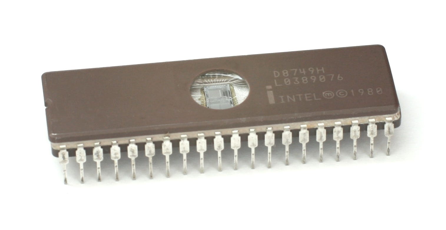
Leading the way, as planned, was the EPROM version, the 8749 with 2K-Bytes of EPROM memory.
And the decision to launch with the EPROM version soon paid off:
… the beauty of the product was you could get the product and because it was EPROM capability you could immediately start producing a prototype and that really was probably the 8048's family's best feature. And so anybody who had one of these things, an EPROM programmer, could essentially start doing a product; and people did.
Not only was the 8048 family more versatile than the 4040 it was in a different league to TI’s TMS 1000 microcontroller series. A simple comparison of some of the features and options shows how big a step forward Intel’s designs were:
8-bit (vs 4-bit) registers, arithmetic and data transfers;
8-level stack (vs 1-level);
Expandable externally with more ROM, RAM and Input / Output ports;
UV erasable EPROM version.
The 8048 also avoided lots of the odd features of the TMS 1000 - such as 64 byte paged program memory - and developing systems using the new Intel design would be much more straightforward.
Costs
It was a major advantage for customers to be able to quickly develop working designs. But for the 8048 series to be really successful then it needed to be low-cost. The team set a target of getting the price of (mask programmed) versions to $2.50 at the end of 1978, down from $8.50 at the start of the year.
The main things were yield improvement. At the time the yield was atrocious and-- which was the number one costing factor. And then we went on to convert the product onto four inch wafers, and 8048 was probably the first, or among the first product to be converted onto the four inch wafers, in the Livermore plant.
By the end of 1978, the cost was down to $2.53. For comparison, an 8-bit microprocessor like the Z80 retailed for around $30 and needed lots of support chips to create a working system. The 8048 series would soon find its way into lots of electronics where even an 8-bit microprocessor wouldn’t be cost effective.
It’s worth just pausing for a moment to consider what the semiconductor industry had achieved in less than a decade. In 1970 the cheapest computer cost hundreds of dollars or even thousands of dollars, even excluding the cost of peripherals. By 1978 it was possible to buy a reasonably capable complete 8-bit ‘computer on a chip’ for just $2.53.
Applications
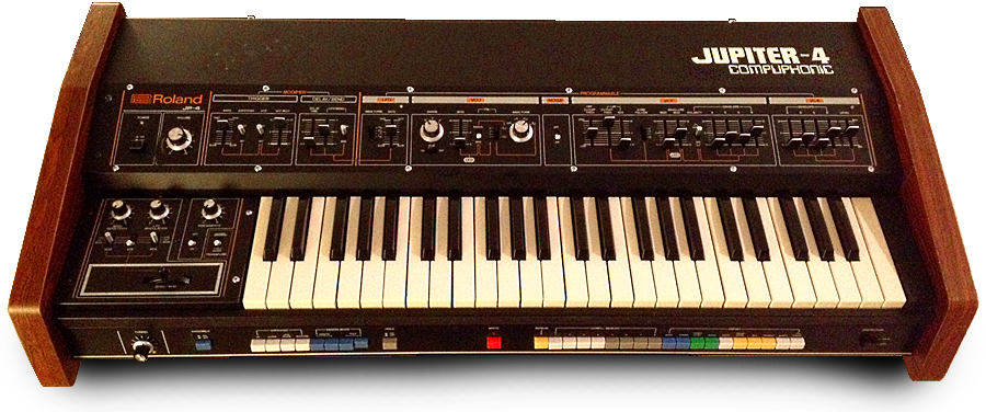
With its low cost, impressive capabilities and rapid time to market, the design wins for the 8048 family started to roll in. From gas pumps to music synthesisers to printers and even video game consoles. The 8048 was powerful enough to take on a wide range of roles.
One important design win was in the original IBM PC keyboard. From the IBM technical manual:
The microprocessor (Intel 8048) in the keyboard performs several functions, including a power-on self-test when requested by the system unit. This test checks the microprocessor (Intel 8048) ROM, tests memory, and checks for stuck keys. Additional functions are keyboard scanning, buffering of up to 16 key scan codes, maintaining bidirectional serial communications with the system unit, and executing the handshake protocol required by each scan-code transfer.
So every IBM PC would ship with not one but two Intel processor architectures!
A small selection of 8048 powered devices:
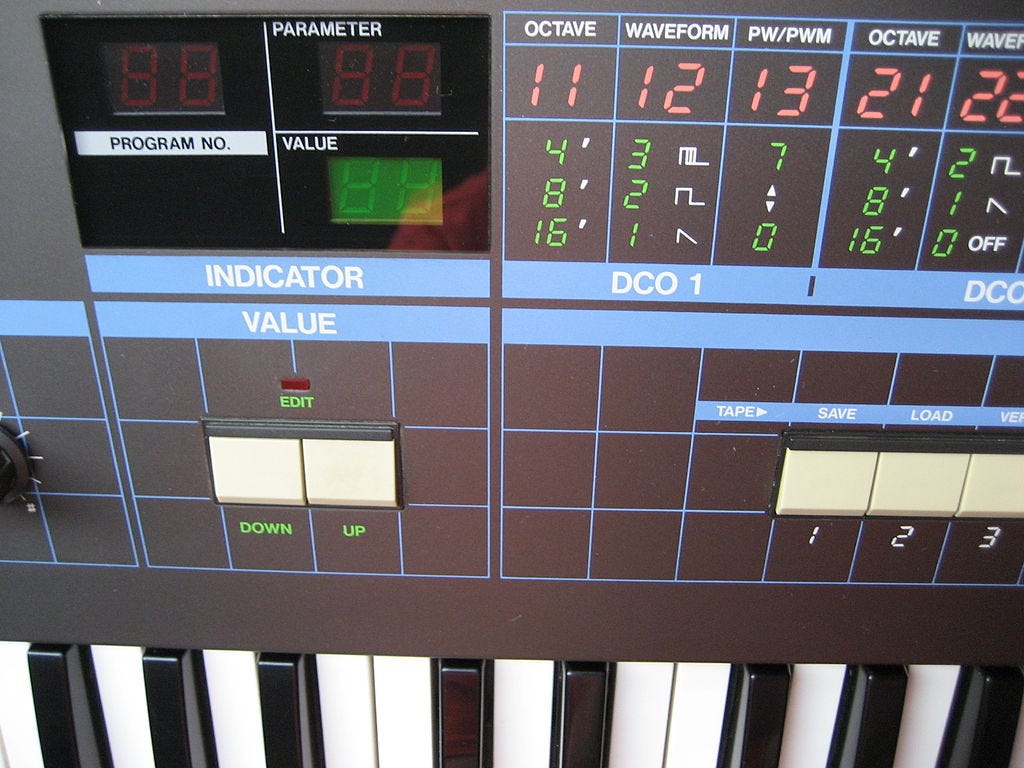
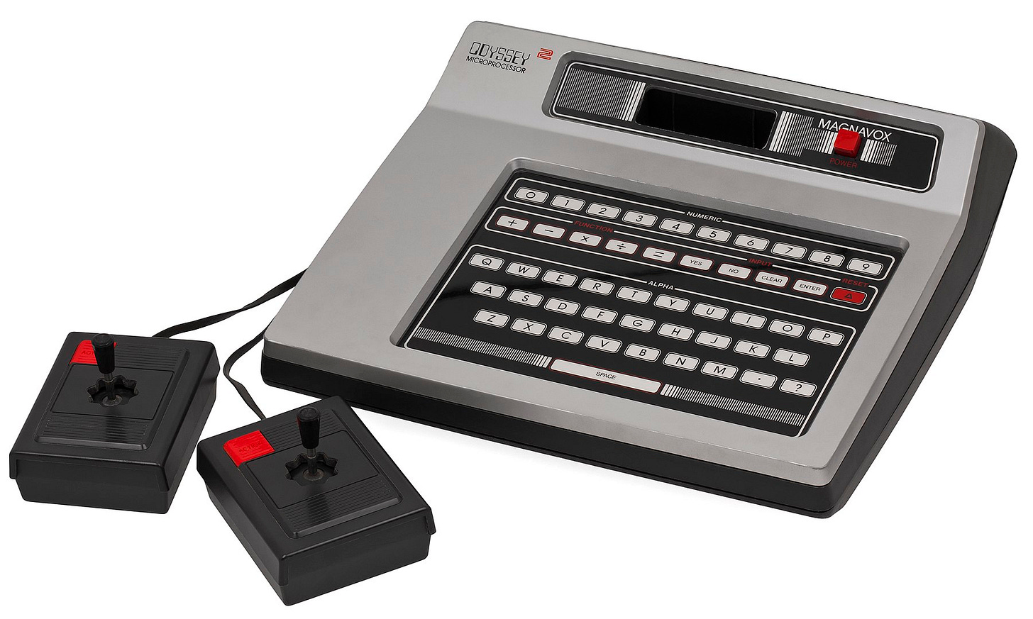
In the last quarter of 1976 Intel shipped just 770 ‘revenue units’ of the 8048 family. But Intel’s microcontroller revenue grew rapidly to $7m in 1977 and reached $70m by 1980. Intel’s total revenue was $800m in 1980, so the brand new microcontroller business made up almost 9% of revenue after just four years.
The success of the 8048 led to it being produced by some ‘second sources’ including some some ‘unofficial’ ones including National Semiconductor, where Howard Raphael had moved after working on the 8048 project at Intel.
And of the course the project that I had National second source was the 8048. So we did an NS8048. It was a non-sanctioned second source. So it was essentially engineered from scratch.
But the limitations of the 8048’s architecture had become apparent early on, through Dave Stamm’s efforts to write a ‘blackjack’ card game program as an initial demonstration of the capabilities of the design:
And so we decided that we were going to try to write a blackjack playing program, all within the 8048. And all we wanted to demonstrate it was two single chips. So we wanted just the chip connected to a dumb terminal, which is a black and white terminal with its own integrated keyboard that could put up little strange little characters so that you could actually form playing cards. And we built this, we were able to do it, we could just fit it in. And I realized some of the limitations of my own instruction set, unfortunately, …
… we had the single chip device connected to the dumb terminal and you could sit there and say hit, stand, double down -- actually I don't think we did double down because that would've meant more complexity and I think I was out of programming space.
The 8048 was also soon starting to see successful competition from Mostek’s 8-bit microcontroller, the 3870. So, as early as December 1977 work started on the development of the successor to the 8048 family, a series of chips that Intel continued making until 2007, and which are still being made by other firms even today. We’ll cover that family and more in the next and final instalment of this series.
After the break, we look at the 8048 series in more detail, with more links, further reading and some of the original documentation.


