The First Intel 'Fab'
Humble beginnings and a toxic legacy
A recent edition of the excellent Asianometry newsletter has a fascinating article and video describing TSMC’s latest ‘Giga-Fab’. The article and the video are both highly recommended.
The latest TSMC Fabs are simply staggering. To quote from the article:
In 2018, TSMC broke ground on Fab 18 near Tainan City in the south of Taiwan. Fab 18 is a monster. It sits on 103 acres and has a total floor space of 950,000 square meters (10.2 million square feet).
and
In total, across all of its phases, Fab 18 will cost TSMC nearly $20 billion to build and operate. More than the cost of the USS Gerald R. Ford, the US Navy's most advanced aircraft carrier.
This prompted me to look into what has happened to Intel’s very first Fab.
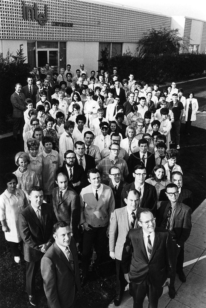
Intel’s first office was at 365 East Middlefield Road in Mountain View. The photo at the top of this article has Intel’s 106 staff standing outside the office in 1969. At the front on the left is Robert Noyce with Gordon Moore on the right. Behind Moore on his left is Andy Grove and behind Moore, wearing glasses, is Ted Hoff.1
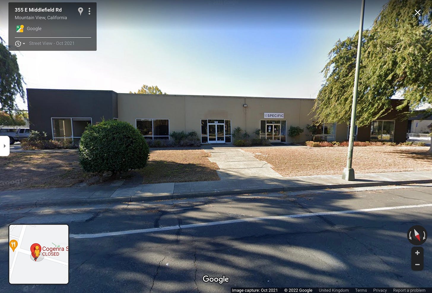
Google Street View gives us a clear view of this building in 2021.
It’s visibly the same building with some minor alterations.
Intel started to move into 365 East Middlefield Road soon after its founding in 1968. Previously a Union Carbide office, Intel first had twelve engineers move into a conference room, whilst Union Carbide moved out. Gordon Moore wondered aloud whether Intel would ever need all the space.
In fact, Intel soon outgrew the, roughly 30,000 square feet, site. A new building was opened in Santa Clara in 1971 and Intel vacated East Middlefield Road in 1981.
Calling the building a Fab is both understating and overstating its role. It housed all of Intel’s operations for a time: manufacturing, design and management. But the scope and sophistication of the manufacturing operations would have been a world away from those of TSMC or Intel today.
At the moment building seems to be unoccupied and to be available on a short-term lease. But not for too much longer. The site and one adjacent to it have approval to be redeveloped for apartments.
It’s interesting how unsentimental Silicon Valley can be. One of its most important companies started here and there seems to be no sign, no commemoration at the site at all.
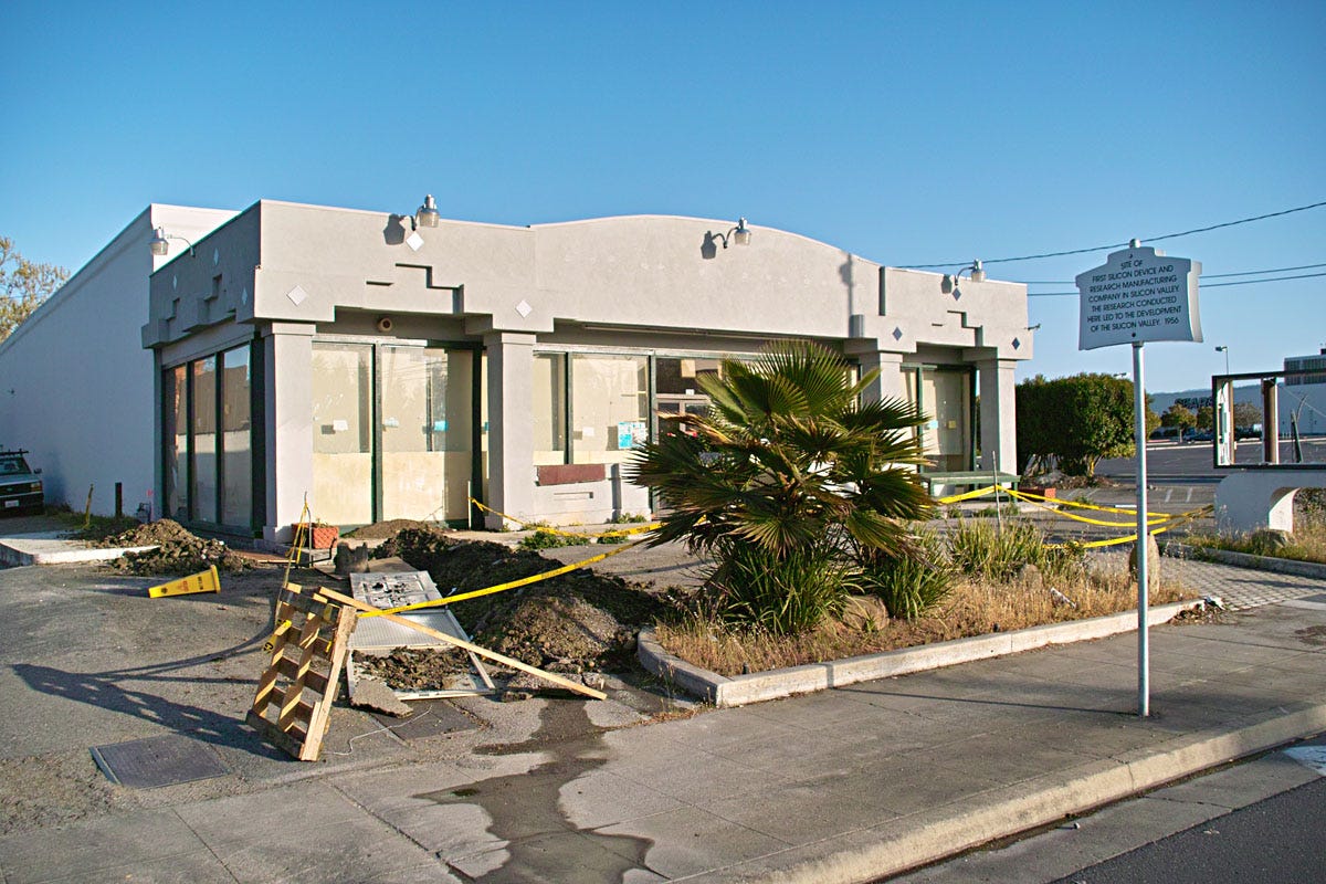
It’s interesting to compare with the site of Shockley Semiconductor Laboratory, not far away at 391 San Antonio Road, seen by many as the birthplace of Silicon Valley in 1955. The site was converted into a retail store but was in a decrepit state by 2007.
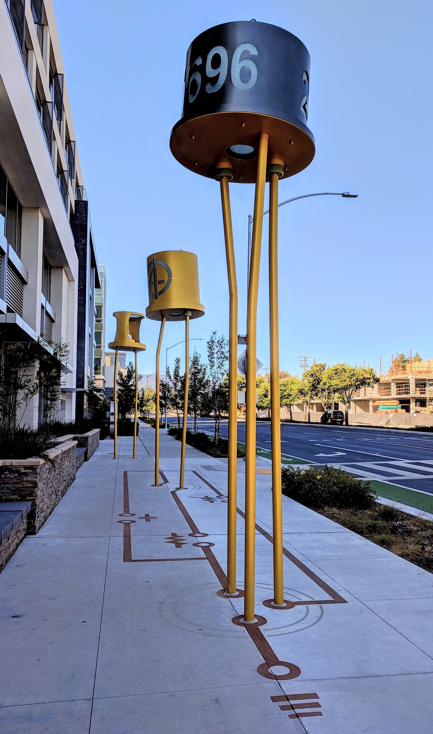
The area has since been redeveloped with offices, some of which are occupied by Facebook. Outside are some giant transistors and diodes on the sidewalk.
A plaque at the location reads:
At this location, 391 San Antonio Road, the Shockley Semiconductor Laboratory manufactured the first silicon devices in what became known as Silicon Valley. Some of the talented scientists and engineers initially employed here left to fund their own companies, leading to the birth of the silicon electronics industry in the region. Hundreds of firms in electronics and computing can trace their origins back to Shockley Semiconductor.
Those talented employees of course included Robert Noyce and Gordon Moore who had joined Shockley here, but soon left to found Fairchild Semiconductor.
The industry has travelled a long way, both literally and metaphorically, since 1955.
The Clean-up
But there is a darker side to fabs. Toxic chemicals from the Intel site have leaked into the surrounding environment at the site. Quoting the Environmental Protection Agency on this site and others nearby:
Site investigations at several of these facilities during 1981 and 1982 revealed significant soil and groundwater contamination by toxic chemicals, primarily volatile organic compounds (VOCs).
Despite the removal of contaminated soil, cleanup of the site will take decades more:
Groundwater cleanup will continue to operate for many decades in order to meet the trichloroethene (TCE) groundwater cleanup standard of 5 parts per billion.
So more than fifty years after the site opened and forty after it closed, its toxic legacy lives on. For all that semiconductor manufacturing is ‘high tech’ it’s hard to ignore that it is an industry with a serious environmental impact.
Image Credits
Intel Building
Intel Free Press
Attribution-ShareAlike 2.0 Generic(CC BY-SA 2.0)
https://www.flickr.com/photos/intelfreepress/8226808663/in/album-72157631636918757/
Shockley Building
CC BY-SA 3.0
https://en.wikipedia.org/w/index.php?curid=10570258
Shockley Transistors
Dicklyon
CC BY-SA 4.0
https://creativecommons.org/licenses/by-sa/4.0, via Wikimedia Commons
I have no idea who the gentleman who is circled on the photo. It’s the only version which has a useable Creative Commons license.


Loved this newsletter. The history of Intel is really very intriguing, the giant diodes and transistors looked good 😂