Intel Everywhere
The Story of the Intel 8051 Series - Part 1

One way of thinking of the 8051 when it was launched is as the most powerful ‘System-on-Chip’, the Apple M1 of its era.
This is the third installment of our series on early microcontrollers. Previously, in Tiny Computers from Texas, we’ve seen the very first microcontrollers, created by Texas Instruments at the start of the 1970s, then in Intel’s Inside, we discussed the first microcontroller designs from Intel, the 8048 series.
I say ‘early microcontrollers’ but today’s post is about a microcontroller design that, although it appeared over forty years ago, is still very much around today. In the intervening decades, billions or maybe even tens of billions of devices using the design have been shipped. I’m reasonably sure that just about everyone reading this will have, possibly unknowingly, used a device containing one of these designs.
It’s Intel’s MCS-51 family, now usually just called ‘the 8051’.
The longevity and the ubiquity of the 8051 series begs several questions. Why has it been so successful? What is it about the 8051 that has given it such longevity? Why has it not been replaced by more modern designs?
The success of the 8051 is even more striking given its humble origins. The design was the brainchild of a young engineer who only got to propose his ideas because he’d forgotten his wallet and was invited to share a lunch by his fellow Intel engineers. That man, John Wharton, would have a fascinating career that led the New York Times to say he had a ‘Zelig-like’1 presence in Silicon Valley.
In a moment we’ll look at the ‘origin story’ of the 8051. A second post on the 8051 will look at the design's key features and try to answer the questions we’ve posed above. First, though let’s try to put the 8051 into some historical context.
In December 1982, Byte magazine ran an article introducing readers to the new Intel design. The article started with a striking introduction.
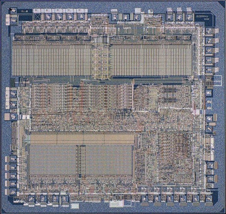
Intel claims that the MCS-51 family is the “highest performance microcomputer family in the world and outperforms all microprocessors and microcomputers in control-oriented applications.” It achieves a tenfold function/speed improvement over its predecessor, Intel's 8048, by packing 60,000 transistors onto a silicon die about 230 mils square.
Byte mentions three members of the MCS-51 family, all with 128 bytes of RAM:
8031 - No internal ROM
8051 - 4k Mask Programmable ROM
8751 - 2k Erasable Programmable ROM (EPROM)
If Intel claimed the title “Highest performance microcomputer family in the world” then that was highly questionable. In 1982 many users were transitioning from 8-bit to 16-bit microcomputers and microprocessors. 8-bit designs like the Z80 and the 6502 were still widely used. However, 16-bit designs like Intel’s 8086 (launched in 1977) and Motorola’s 68000 (1979) had already been on the market for a while and the 8088-based IBM PC had launched in 1981.
The performance of the 8051 series couldn’t approach that of the 8086 or the 68000. But, the 8051 wasn’t designed to compete with these designs. Instead, it was intended to provide enough processing power for common control applications in a single package.
If today we often think of the 8051 as a ‘tiny’ design, in 1982, physically at least, it was anything but. The 60,000 transistors of the 8051 compares to around 29,000 in the Intel 8086. One way of thinking of the 8051 when it was launched is as the most powerful ‘System-on-Chip’, the Apple M1 of its era.
How did Intel come to develop the 8051? It’s a fascinating story combining happenstance, the brilliant contribution of one outstanding engineer, and the power of Intel’s early corporate culture. In telling the story, we’ll quote liberally from the excellent Intel 8051 Microprocessor Oral History Panel. The story starts with the search for a successor to the 8048.
The Development of the 8051 Series
Intel launched the 8048 series in the last quarter of 1976 with one key advantage over competition from TI and others: an ‘Erasable Programmable ROM’ (EPROM) variant:
… the beauty of the product was you could get the product and because it was EPROM capability you could immediately start producing a prototype and that really was probably the 8048's family's best feature. And so anybody who had one of these things, an EPROM programmer, could essentially start doing a product; and people did.
By 1977 production and sales of the 8048 series were ramping up and Intel had proven that there was a market for these designs. Microcontroller sales would reach $70m in 1980, around 8% of Intel’s total revenues, and these sales were growing faster than the company as a whole.
However, the limitations of the 8048 architecture became clear very quickly. Critically, it had a 2k-byte address space with an awkward ‘bank-switching’ approach used to expand to 4K.
The series had a maximum of 4K-Bytes of program memory with a 12-bit program counter. This memory was arranged into two banks of 2K-Bytes and a bit set with a special instruction ‘SEL’ would determine which bank a jump (JMP) or subroutine call instruction (CALL) would point to.
So the question was how to expand the capabilities of Intel’s microcontroller series. The situation was complicated by the success of Intel’s 8-bit microprocessors, the 8080 and 8085.
… within Intel, we were really wrestling with how far would you take the processing power of this kind of class of product. Obviously, it didn’t make sense for Intel to have competing architectures for the same applications. The 8080 and 80X later became the 86 or x86 family of products.
If using a variant of Intel’s microprocessor series wasn’t an option then what would the 8048’s successor look like? The answer came from a surprising source.
John Harrison Wharton

John Harrison Wharton had completed his Master’s degree in Computer Science at Northwestern University in 1977 having moved there from Yale two years earlier. He immediately joined Intel in Santa Clara and started designing systems using the 8048 microcontroller and the 8085 microprocessor. By the end of 1977 Wharton was working in a group trying to get a ‘foot in the door’ for Intel in firms and industries that they believed would be important. According to Wharton:
… the way they were doing that was by finding about some major design that was in the works, [such as] a new microwave oven or an electronic engine control for Ford automobiles. And my group would quickly prototype a demonstration of that application using Intel processors instead of discrete circuitry or competing processors. The important thing there was for us to try to do designs within a month or so and demonstrate something and then be done with it.
One morning in mid-December 1977, Wharton left his wallet at home, so he asked his manager Lionel Smith if he would take him to lunch. Wharton recalled that this led to an invitation to a lunch meeting.
And he said, “Well, I can’t today because I have to go to a, what they called a lunch bunch. “I have to go a lunch-time planning meeting.” But he said, “They always have sandwiches there and there’s always food left over so why don’t you just come along and you can hide in the back and nibble on whatever is left?”
One of the topics under discussion was the future of the 8048 series. Wharton recalled the approach that had characterized the architecture so far.
… there was sort of a mindset in that era that you’d figure out what the hardware facilities would be and then almost as an afterthought come up with an instruction set that gives you sufficient access to all of the things that the chip designers provided.
The evolution of the 8048 series had involved ‘tweaking’ earlier versions to accommodate additional hardware. Each successive version was incompatible and harder to use than the previous one. Even worse, this led to a proliferation of instruction sets.
By this time there were about eight or nine different offshoots of the 8048, no two of which had exactly the same instruction set.
All the proposals discussed over lunch continued with this approach. Wharton could see how problematic this was and that this would soon run up against some hard limits beyond which it would be difficult to evolve the 8048 architecture further. After lunch, Wharton returned to his cubicle and started sketching his ideas for a better approach. The next day he had his regular ‘one-on-one’ meeting with Smith who asked him what he thought of the lunch meeting. Wharton shared his concerns about the discussions, so Smith asked him to propose a more flexible architecture. It didn’t take long.
… I tried to summarize the issues that needed to be resolved over the weekend. Wrote up a proposal for a combination of instructions and addressing modes that would take care of that. Brought that in Monday morning to discuss with Lionel …
What was different when compared to the 8048?
The main thing that I did was introduce the idea of separating the processor capabilities from the IO capabilities. Until that point every processor Intel had introduced had made changes to the earlier processors’ instruction sets -- and this was the right thing to do.
Smith added Wharton’s proposal to half a dozen already under consideration. In some corporate cultures, a proposal from outside the 8048 group, from an inexperienced 23-year-old engineer, would not have been received well. Intel was different though.
Intel has a culture of constructive confrontation, and people were doing that quite actively to each other. I found throughout the rest of my career that that was an extremely valuable element of the culture. But [with] all these different architectures and about six or seven different alternatives on the table and now with John’s on the table as well.
How to decide between the alternative approaches, including Wharton’s more radical departure from the 8048 series? Wharton’s ideas had quickly won over some colleagues.
And I think we got John’s proposal, I would guess as early as Tuesday, and it was a thing of beauty. It was really an aesthetic thing to look at compared with some of the stuff we had left over.
A more rigorous approach was needed for the final decision though. For that, the team looked at earlier work that had taken …
… an intense look at the telecommunications industry, the automotive industry, the consumer appliance industry, the computer peripheral industry. Out of this came a range of applications you want to get into, what are the features you would need or the functions you would need on a single chip or a couple of chips, to really do that more cost effectively. And so what we did was to say, “Look here are the ones that we see as the biggest opportunities. Here are the growth rates. How do each of these alternatives really map into that?”
It quickly became clear that Wharton’s proposal was the best fit for these applications and got the team out of the ‘quagmire’ of continually changing the instruction set.
Andy Grove is reported to have said about Intel that ‘It’s a dictatorship that believes in the First Amendment’. So everyone had their say, but after the decision was made Intel’s ‘disagree and commit’ rule applied, and the team started building the new design according to Wharton’s proposals.
Moving to Arizona
We saw in Leaving Arizona that Motorola moved the team developing the 6800 microprocessor series from (Phoenix) Arizona to Texas in 1975. By the end of the 1970s, Intel was also moving teams to the East, to Arizona, not like Motorola to cut costs, but instead to support expansion.
We were doubling revenue each year and showing that there was definitely a key market for this kind of technology and we could exploit that in a much bigger way. … we couldn't grow quickly enough in the Bay area, so the move to Arizona was planned for this operation. … And we knew we needed to expand more quickly. We needed to move the group to Arizona in this case.
The 8051 was ‘taped out’ in Santa Clara, at the end of 1979, before most of the development team - apart from John Wharton who stayed in California - moved to Arizona. This was probably a good decision as continuing development in Phoenix wasn’t straightforward.
No one had PCs. A couple of people had Apple IIs, but they were only using them on their own. We had to communicate by people typing on IBM Selectric typewriters with orator type and foils and you have to jump on a plane and schlep those back and forth between Phoenix and Santa Clara. … the design, a lot of it was still on pen and paper red lining or yellow lining, checking off different schematics. So if the audience is thinking in terms of, "Well, working remotely, that's no big deal, that's routine," it was much, much more challenging to do it in that era than it was today.
And there were challenges because of the newness of the operations in Arizona:
… it was very much what I would call guerrilla engineering. I mean, there was no support infrastructure in Arizona. And from a manufacturing sense, I mean, if you smashed your probe card there was no probe card repair group in Arizona. You had to figure out how to get things done.
The team had to design versions of the 8051 design with ROM and EPROM most of the design was common across the two variants.
… it was fortunate we didn’t have to focus a lot of time on developing either the ROM or EPROM circuitry. Just leave spaces on the chip at least for the ROM version. The EPROM version was much larger than that but required a modification to the layout to push one side out far enough to support the EPROM core.


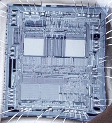
If we zoom in on the exposed 8751 chip in the package above and compare it with the die shot of the 8051 at the top of this post we can see the similarities in the layout at the bottom of the chip, but the significant difference between the ROM and the larger EPROM at the top of the die.
Making the 8051
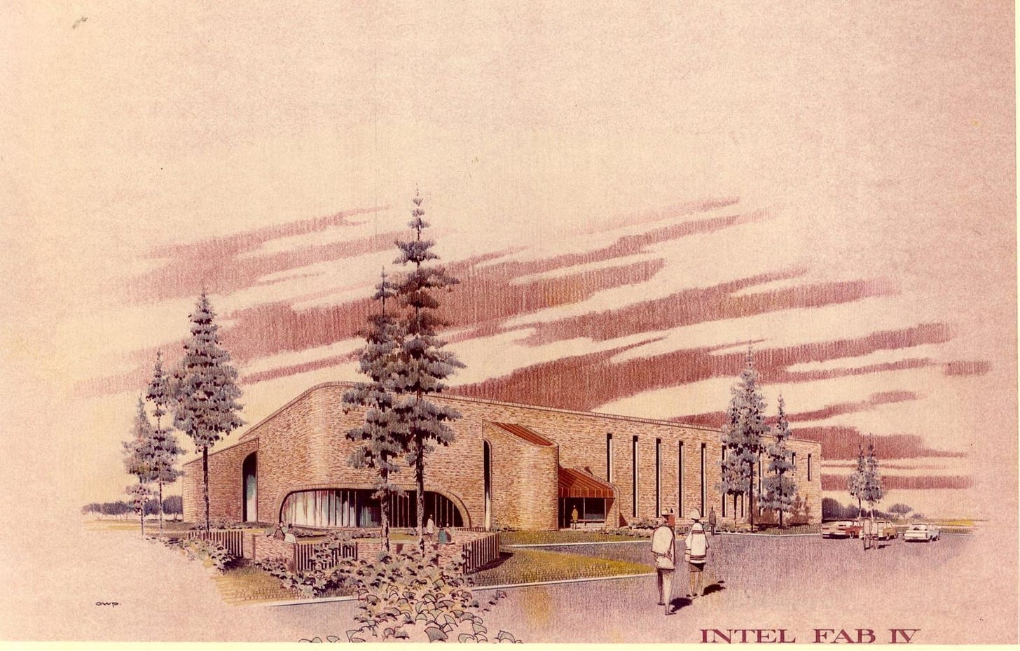
If the development of the 8051 had been moved East then production of the new design was headed North. Intel would build a Fab in Chandler but it would not be operational until 1980 so early 8051s would be built in Oregon at Intel’s Fab 4.
The combination of the work at Fab 4 and the efforts of the team that designed the 8051 led to some remarkably high yields.
I do believe on that level of technology that the 8051 produced in Fab 4 was the first fully functional wafer ever produced by Intel. … a hundred percent yield on a wafer and running final test yields in the 99.5 percent range was pretty darn good for a product in those days.
Performance 8051 vs 8048
How did the performance of the 8051 compare with its predecessor? At the 8051’s launch in 1980, Intel provided a chart comparing die size and performance.
The 8051 offered up to 10x the performance of the 8048 with 1.4x the die size.
Early Use of the 8051
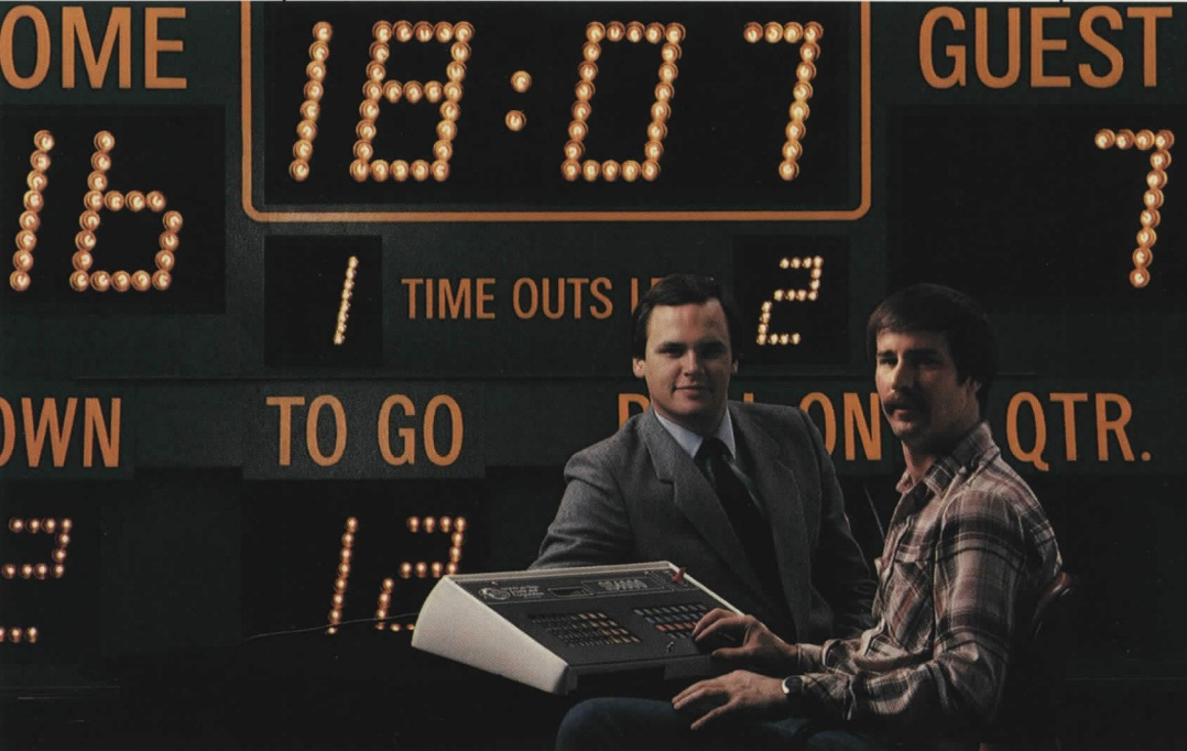
The introduction of the 8051 was important enough to feature in Intel’s 1981 Annual Report, which featured probably one of its higher-profile early uses: controlling the electronic display of results at sports venues.
"One of the first products on the market incorporating Intel's new 8051 single chip microcomputer is American Sign & Indicator's SS4000 electronic scoring console. We've been working closely with the company to develop the 8051-based controller for the system, which allows American Sign to build a very powerful and versatile scoring console with the minimum number of chips possible. The 8051's internal timers and expansion memory capabilities allow American Sign to put the scoring programs of 5-6 sports in one console. These scoring consoles are designed for use by high schools, colleges and professional sport stadiums."
This was just the start for the 8051 series though. We’ll look at more uses and its later history in the next post along with a detailed look at the architecture of the 8051 series.
In the meantime, premium subscribers who want to know more about the 8051’s architecture can download the 1982 Byte magazine article below.


